
Integrated bootstrap high voltage driving chip and technological structure thereof

A high-voltage drive chip, high-voltage technology, applied in the field-effect transistor logic circuit coupling/interface, pulse technology, diodes, etc., can solve the problems of increased chip area, bootstrap capacitor leakage, large on-resistance, etc., to achieve reduction The effect of small chip area, simplified circuit structure, and small conduction voltage drop

Active Publication Date: 2016-08-03
SOUTHEAST UNIV +1
View PDF9 Cites 23 Cited by
  • Summary
  • Abstract
  • Description
  • Claims
  • Application Information

AI Technical Summary

Problems solved by technology

[0003] Using an external bootstrap diode D B The traditional half-bridge drive circuit has obvious disadvantages: the external discrete device bootstrap diode D B It will increase the extra cost of the circuit and increase the complexity of the system; the high-voltage bootstrap diode has a high conduction voltage drop, which will eventually affect the capacitor C B The charging voltage on the upper, and the higher the diode withstand voltage, the greater the conduction voltage drop; the bootstrap diode D B The reverse recovery current will cause the leakage of the bootstrap capacitor
However, the bootstrap diode analog circuit used in the above patents, the added high-voltage power switching device LDMOS and its control circuit greatly increase the complexity of the circuit, and the chip area is greatly increased, and the cost is also increased; Compared, the on-resistance of LDMOS devices is relatively large, which seriously reduces the charging speed of the bootstrap circuit, which makes this technical solution not suitable for some applications, such as high-frequency half-bridge drive circuits

Method used


Image

  • Integrated bootstrap high voltage driving chip and technological structure thereof
  • Integrated bootstrap high voltage driving chip and technological structure thereof
  • Integrated bootstrap high voltage driving chip and technological structure thereof

Examples


Embodiment Construction

[0043] see image 3 , the process structure of the integrated bootstrap high-voltage driver chip of the present invention includes a base 101 of the first doping type, a buried layer 102 of the second doping type, a well 103 of the second doping type and a well 104 of the first doping type Low basin; first doping type well 105, second doping type buried layer 106, first doping type body contact 107, second doping type source contact 108, second doping type drain contact 109, gate High-voltage switch tube composed of electrode 110 and second doping type well 111; high basin composed of second doping type buried layer 112, second doping type well 113 and first doping type well 114; low basin and high voltage switch The source of the tube is close, and the high basin is close to the drain of the high-voltage switch tube. At least one second doping type well 103 and at least one first doping type well 104 are arranged in the lower basin, and the first doping type well 104 is alwa...


PUM


Abstract

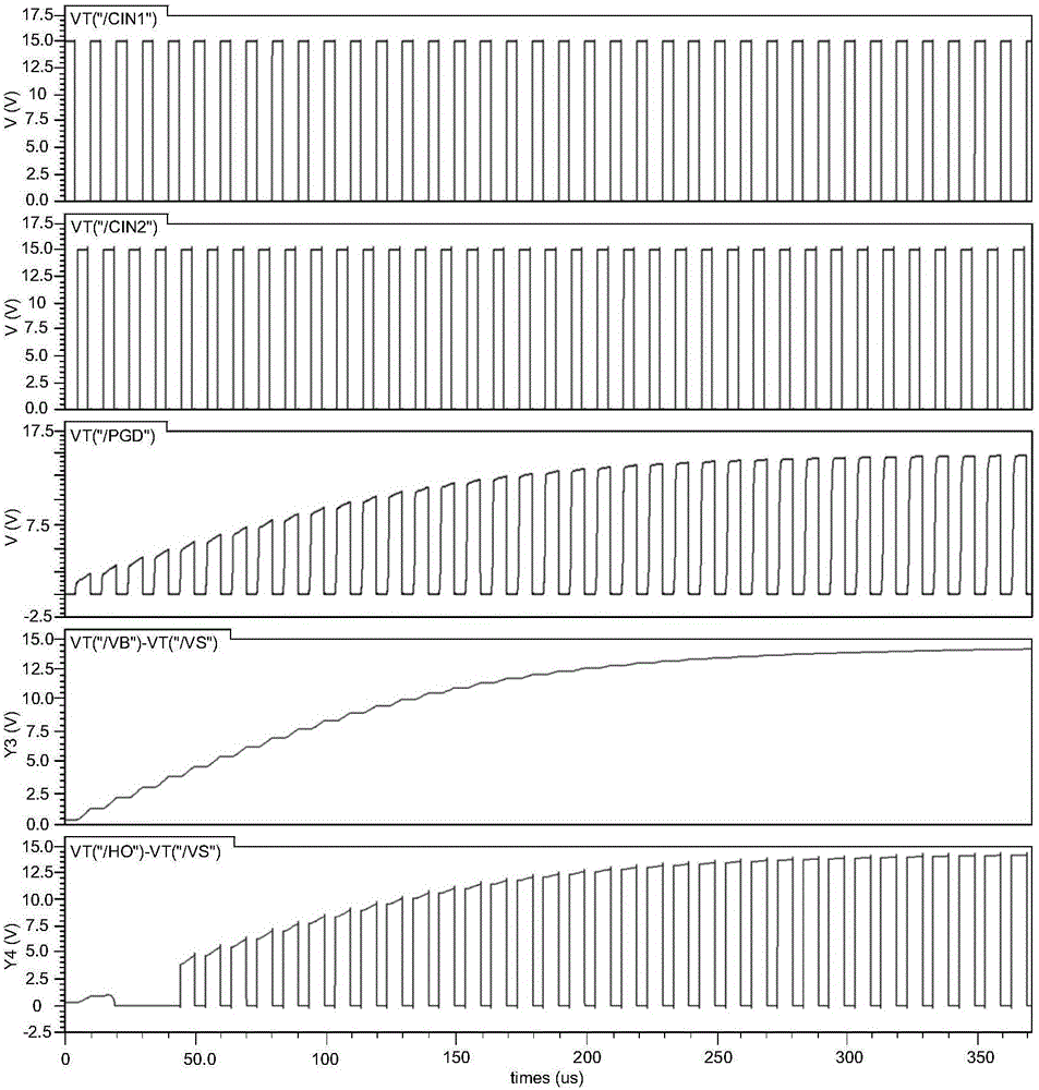
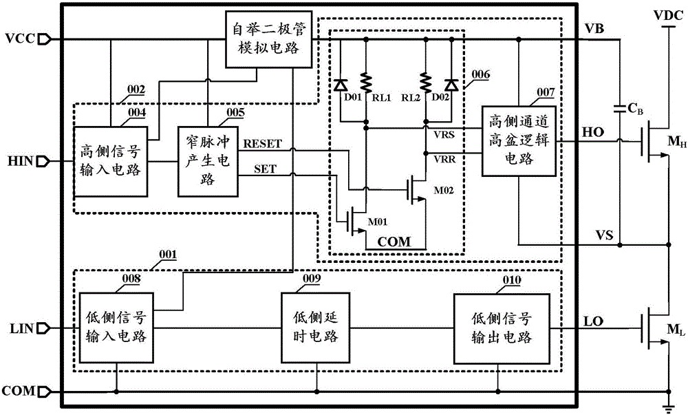
The invention discloses an integrated bootstrap high voltage driving chip and a technological structure thereof. Parasitic high voltage diodes realized by the integration technology in a high voltage level shift circuit are ingeniously utilized to charge a bootstrap capacitor, wherein the power terminal of the high voltage level shift circuit is a high side floating power supply VB, and the reference ground is floating voltage PGD. The PGD is controlled by a bootstrap control circuit. A first parasitic diode and a second parasitic diode are arranged between the VB and the PGD. The bootstrap control circuit is controlled by a high side signal and a low side signal. When the low side output signal LO is high level and the high side output signal HO is low level or the low side output signal LO is low level and the high side output signal HO is low level, the output PGD of the bootstrap control circuit is high level VCC. The VCC performs unidirectional charging to an external bootstrap capacitor through the first parasitic diode and the second parasitic diode. The integrated bootstrap high voltage driving chip is high in charging speed, high in charging efficiency, simple in circuit structure and low in cost.

Description

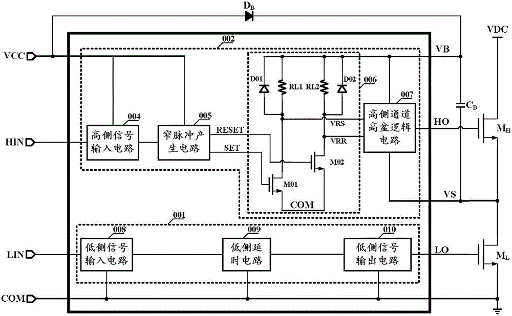
technical field [0001] The invention relates to a bootstrap technology in a half-bridge drive circuit, in particular to an integrated bootstrap high-voltage drive chip and its process structure. Background technique [0002] The half-bridge drive circuit is widely used in the fields of motor drive, electronic ballast, switching power supply, etc. It is used to drive two power switching devices connected in the form of totem poles to make them conduct alternately. Such as figure 1 As shown, the traditional half-bridge driver chip includes a low-side channel logic circuit and a high-side channel logic circuit, wherein the low-side channel logic circuit includes a low-side signal input circuit, a low-side delay circuit and a low-side signal output circuit, and the high-side channel The logic circuit includes a high-side signal input circuit, a narrow pulse generation circuit, a high-voltage level shift circuit and a high-side channel high-basin logic circuit. The high-voltage ...

Claims


Application Information

Patent Timeline
Patent Type & Authority Applications(China)
IPC IPC(8): H03K17/687H01L29/78
CPCH01L29/7818H03K17/687H03K19/0185H03K2217/0063H03K2217/0081H01L29/42368H01L27/0727H01L29/7835H01L29/1083H03K17/063H03K17/162H03K17/6871
Inventor 孙伟锋张允武禹括祝靖徐申钱钦松刘斯扬陆生礼时龙兴
Owner SOUTHEAST UNIV
Learn More