
Flexible copper grid base transparent conducting thin film

A technology of transparent conductive film and copper mesh grid, which is applied to the conductive layer on the insulating carrier and other directions, can solve the problems of difficult to obtain high transmittance and low resistance transparent conductive film, low composite transmittance, etc., and achieve production costs. The effect of low, high transmittance, strong environmental resistance performance

Active Publication Date: 2016-08-10
AVIC BEIJING INST OF AERONAUTICAL MATERIALS
View PDF6 Cites 4 Cited by
  • Summary
  • Abstract
  • Description
  • Claims
  • Application Information

AI Technical Summary

Problems solved by technology

However, since the transmittance in the visible light region of the general transparent substrate PET itself is lower than 92%, after the copper grid conductive layer is prepared on this PET transparent substrate, its composite transmittance is lower, and it is difficult to obtain high Transparent Conductive Film with Transmittance and Low Resistance

Method used


Image

  • Flexible copper grid base transparent conducting thin film
  • Flexible copper grid base transparent conducting thin film
  • Flexible copper grid base transparent conducting thin film

Examples


Embodiment 1

[0027] like figure 1 As shown, this figure shows an embodiment of a flexible copper grid base transparent conductive film, and the composite film includes a flexible transparent polyethylene terephthalate (PET) substrate film 1, which reduces reflection and anti-reflection layer 2 and copper grid conductive layer 3.

[0028] The transparent film substrate 1 is composed of flexible transparent polyethylene terephthalate and its double-sided UV-cured polyacrylate hard coating. Preferably, the thickness of the flexible transparent substrate 1 is 50 microns, and may also be 125 microns. The UV-cured polyacrylate hardening coating is evenly coated on both sides of the flexible transparent PET substrate by a traditional roll-to-roll coating method, so as to improve the strength, hardness and durability of the flexible transparent substrate 1 .

[0029] The anti-reflection and anti-reflection layer 2 is a multi-layer stacked structure, covering the surface layer of the flexible tra...

Embodiment 2

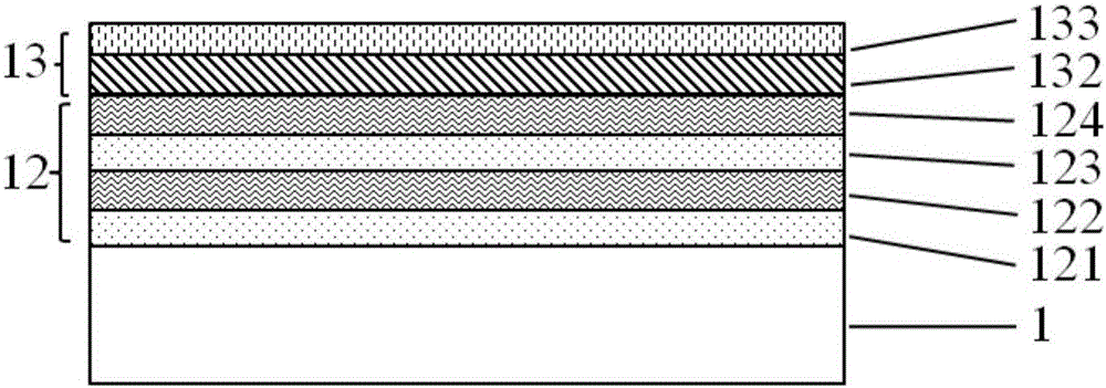
[0032] like figure 2 As shown, this figure shows an embodiment of a flexible copper grid-based transparent conductive film, and the composite film includes a flexible transparent polyethylene terephthalate PET substrate film 1, anti-reflection and anti-reflection layer 12 And copper grid conductive layer 13.

[0033] The transparent film substrate 1 is composed of flexible transparent polyethylene terephthalate and its double-sided UV-cured polyacrylate hard coating. Preferably, the thickness of the flexible transparent substrate 1 is 50 microns, and may also be 125 microns. The UV-cured polyacrylate hardening coating is evenly coated on both sides of the flexible transparent PET substrate by a traditional roll-to-roll coating method, so as to improve the strength, hardness and durability of the flexible transparent substrate 1 .

[0034] The anti-reflection and anti-reflection layer 12 is a multi-layer stacked structure, covering the surface layer of the flexible transpare...

Embodiment 3

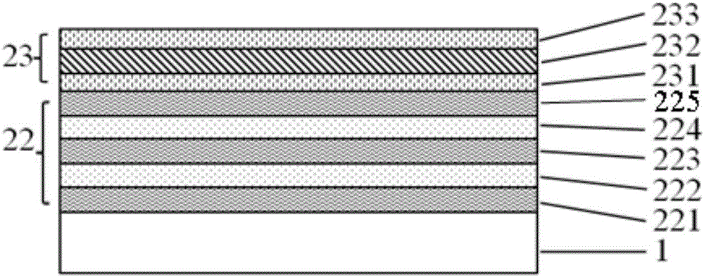
[0038] like image 3 As shown, this figure shows an embodiment of a flexible copper grid-based transparent conductive film, and the composite film includes a flexible transparent polyethylene terephthalate PET substrate film 1, anti-reflection and anti-reflection layer 22 And copper grid conductive layer 23.

[0039] The transparent film substrate 1 is composed of flexible transparent polyethylene terephthalate and its double-sided UV-cured polyacrylate hard coating. Preferably, the thickness of the flexible transparent substrate 1 is 50 microns, and may also be 125 microns. The UV-cured polyacrylate hardening coating is evenly coated on both sides of the flexible transparent PET substrate by a traditional roll-to-roll coating method, so as to improve the strength, hardness and durability of the flexible transparent substrate 1 .

[0040] The anti-reflection and anti-reflection layer 22 is a multi-layer stacked structure, covering the surface layer of the flexible transparen...


PUM

PropertyMeasurementUnit
widthaaaaaaaaaa
thicknessaaaaaaaaaa
thicknessaaaaaaaaaa

Abstract

The invention relates to the field of optical films, in particular to a flexible copper grid base transparent conducting thin film. The flexible copper grid base transparent conducting thin film comprises a flexible transparent thin film substrate, an anti-reflection layer and a copper grid conducting layer, wherein the anti-reflection layer is arranged between the flexible transparent thin film substrate and the copper grid conducting layer. The anti-reflection layer is formed by alternatively overlapping at least one low refractive index film layer and one high refractive index film layer, and the copper grid conducting layer is formed by a diamond or square or hexagonal copper line and at least one cupric oxide thin film layer. The flexible copper grid base transparent conducting thin film can be taken as a substitute of an ITO (Indium Tin Oxide) conducting thin film and is widely applied to the touch screen, flexible display and electromagnetic shielding fields; in comparison with the conventional ITO conducting thin film, the flexible copper grid base transparent conducting thin film has lower production cost, higher transmittance and better anti-oxidation property and at least one order of magnitude higher surface square resistance, and is especially suitable for preparation of large-area high-resolution touch screens.

Description

technical field [0001] The invention relates to the field of optical films, in particular to a flexible copper grid-based transparent conductive film. Background technique [0002] Transparent conductive films are an essential component in the manufacture of devices such as flat-screen TVs, touch screens, smart window panes, light-emitting diodes, and photovoltaic cells. In recent years, with the development of information (such as touch display), energy (such as photovoltaics, smart window glass) and other industries, people's demand for transparent conductive films has increased sharply, and among transparent conductive films, the most widely used The second type is tin-doped indium oxide thin film, commonly known as ITO thin film. As we all know, the content of indium in the earth's crust is rare (about 0.05ppm), and it is difficult to purify. With the significant increase in the amount of ITO thin film, its content is getting rarer and rarer, resulting in a sharp increa...

Claims


Application Information

Patent Timeline
Patent Type & Authority Applications(China)
IPC IPC(8): H01B5/14
CPCH01B5/14
Inventor 刘宏燕颜悦望咏林伍建华张官理
Owner AVIC BEIJING INST OF AERONAUTICAL MATERIALS
Learn More