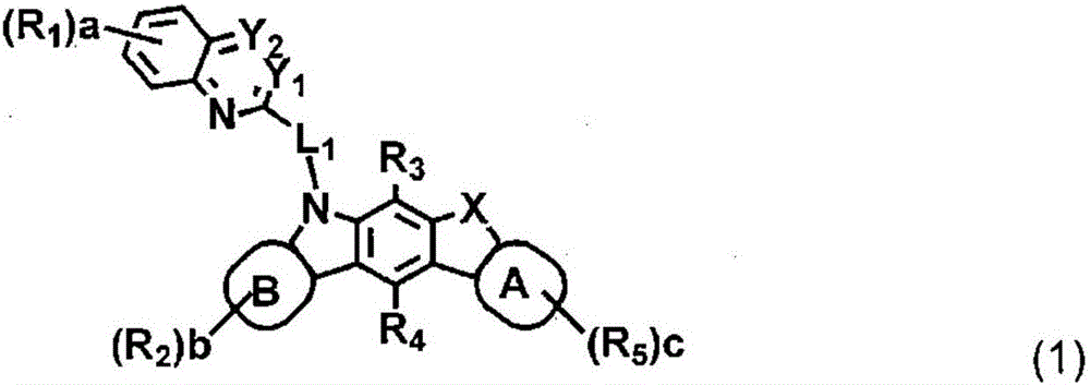
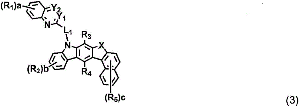
Novel organic electroluminescent compounds and organic electroluminescent device comprising the same

An electroluminescent device and compound technology, applied in electroluminescent light sources, organic chemistry, electric light sources, etc., can solve the problems of low glass transition temperature, decomposition, no advantages, etc., and achieve high luminous efficiency and excellent service life. Effect

Active Publication Date: 2016-08-10
ROHM & HAAS ELECTRONICS MATERIALS LLC
View PDF8 Cites 8 Cited by
  • Summary
  • Abstract
  • Description
  • Claims
  • Application Information

AI Technical Summary

Problems solved by technology

[0007] Although these phosphorescent host materials provide good luminescent properties, they have the following disadvantages: (1) Due to their low glass transition temperature and poor thermal stability, they may decompose during high-temperature deposition under vacuum
Therefore, organic EL devices using conventional phosphorescent host materials do not have an advantage in terms of power efficiency (lm / W)
(3) In addition, the operating life and luminous efficiency of organic EL devices are not satisfactory
However, the power efficiency, luminous efficiency, service life, etc. of organic EL devices including the compounds described in the above publications are still unsatisfactory.

Method used


Image

  • Novel organic electroluminescent compounds and organic electroluminescent device comprising the same
  • Novel organic electroluminescent compounds and organic electroluminescent device comprising the same
  • Novel organic electroluminescent compounds and organic electroluminescent device comprising the same

Examples


example 1

[0103] Example 1: Preparation of Compounds H-61, H-60, H-10 and H-11

[0104]

[0105] 1) Preparation of Compound 1-1

[0106] Compound A (100.0 g, 356.0 mmol), 1-naphthylboronic acid (51.0 g, 297.0 mmol), tetrakis(triphenylphosphine) palladium(0) (Pd(PPh 3 ) 4 ) (11.0g, 9.0mmol), 2M K 2 CO 3 (500.0 mL), toluene (1000.0 mL) and ethanol (500.0 mL) for 5 hours. After completing the reaction, extract with ethyl acetate (EA) and pass through with MgSO 4 The organic layer was dried by removing residual moisture. The residue was separated by column chromatography to obtain Compound 1-1 (70.0 g, 72%).

[0107] 2) Preparation of compound 1-2

[0108] Compound 1-1 (70.0 g, 213.0 mmol), triphenylphosphine (140.0 g, 533.0 mmol) and dichlorobenzene (1.0 L) were dissolved in a flask, and the mixture was refluxed at 150° C. for 6 hours. After completing the reaction, the mixture was distilled and triturated with methanol (MeOH) to obtain compound 1-2 (40.0 g, 64%).

[0109...

example 2

[0135] Fabrication of OLED devices using organic electroluminescent compounds according to the invention

[0136] An OLED device was fabricated in the same manner as in Device Example 1 except that Compound H-60 ​​was used as a host in the light emitting material.

[0137] The fabricated OLED device exhibited a brightness of 1050 cd / m at 3.4V 2 red light and a current density of 8.2mA / cm 2 . Furthermore, the time taken for the brightness at 5,000 nits to drop to 90% of the brightness is at least 130 hours.

example 3

[0139] Fabrication of OLED devices using organic electroluminescent compounds according to the invention

[0140] An OLED device was fabricated in the same manner as in Device Example 1 except that Compound H-10 was used as a host and Compound D-88 was used as a dopant in the light emitting material.

[0141] The fabricated OLED device exhibited a brightness of 920cd / m at 3.6V 2 red light and a current density of 12.2mA / cm 2 . Furthermore, the time taken for the brightness at 5,000 nits to drop to 90% of the brightness is at least 110 hours.


PUM

PropertyMeasurementUnit
thicknessaaaaaaaaaa

Abstract

The present invention relates to a novel organic electroluminescent compound and an organic electroluminescent device comprising the same. The organic electroluminescent compound according to the present invention can be used in a light-emitting layer and has excellent luminescent efficiency; and an organic electroluminescent device comprising the organic electroluminescent compounds of the present invention has long lifespan, and improved current efficiency and power efficiency.

Description

technical field [0001] The present invention relates to novel organic electroluminescent compounds and an organic electroluminescent device comprising said compounds. Background technique [0002] Electroluminescence (EL) devices are self-luminous devices, which have the advantages of providing wider viewing angles, greater contrast ratios, and faster response times. The organic EL device was first developed by Eastman Kodak by using small aromatic diamine molecules and aluminum complexes as materials for forming the light emitting layer (see Appl. Phys. Lett. 51, 913, 1987). [0003] An organic EL device generally includes an anode, a cathode, and an organic layer formed between the two electrodes, and emits light by recombining holes injected from the anode with electrons injected from the cathode. The organic layer of an organic EL device can be composed of a hole injection layer (HIL), a hole transport layer (HTL), an emission layer (EML), an electron transport layer (...

Claims


Application Information

Patent Timeline
Patent Type & Authority Applications(China)
IPC IPC(8): C07D487/04C07D403/10C07D491/048C07D495/04C09K11/06
CPCC07D403/10C07D487/04C07D491/048C07D495/04C09K11/06H05B33/14H05B33/20C09K2211/1007C09K2211/1011C09K2211/1029C09K2211/1044C09K2211/1059C09K2211/1088C09K2211/1092C09K2211/185C07D491/04H10K50/00
Inventor H-R·康M-J·李H-J·康N-K·金C-S·金B·金Y-J·曹K-J·李
Owner ROHM & HAAS ELECTRONICS MATERIALS LLC
Why Eureka
Try Eureka