A planar grid igbt and its manufacturing method

A technology of planar gate and gate electrode, which is applied in the field of planar gate insulated gate bipolar transistors and insulated gate bipolar transistors, and can solve the problems of reducing device switching speed, device oscillation, electromagnetic radiation, etc.

Inactive Publication Date: 2019-01-29
UNIV OF ELECTRONICS SCI & TECH OF CHINA
View PDF4 Cites 0 Cited by
  • Summary
  • Abstract
  • Description
  • Claims
  • Application Information

AI Technical Summary

Problems solved by technology

The gate structure on the upper part of the wide JFET region brings large device capacitance, especially the gate-collector capacitance, which reduces the switching speed of the device, increases the switching loss of the device, and improves the ability of the gate drive circuit of the device. Require
In addition, the gate capacitance on the upper part of the JFET region of the device will form a negative differential capacitance effect when the device is turned on with a small current, which will cause the device to oscillate during the turn-on process and thus cause electromagnetic radiation problems

Method used


Image

  • A planar grid igbt and its manufacturing method
  • A planar grid igbt and its manufacturing method
  • A planar grid igbt and its manufacturing method

Examples


Embodiment 1

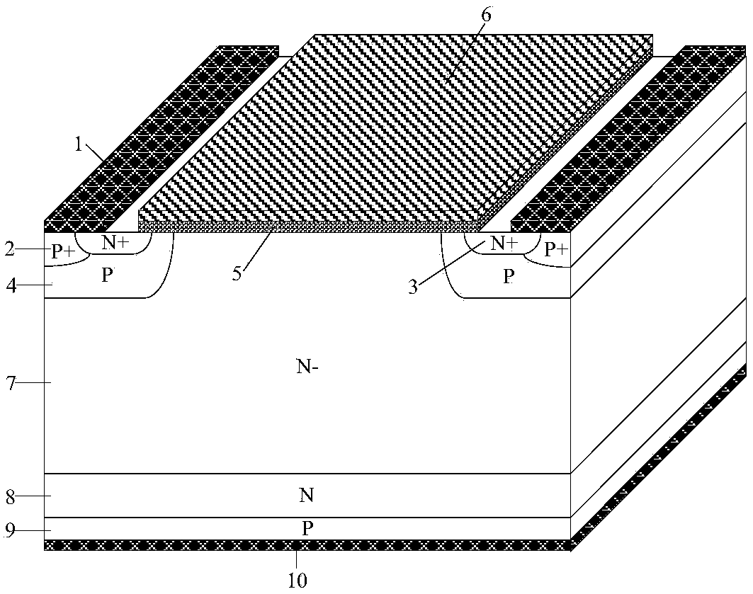
[0045] A planar gate IGBT with a half-cell structure such as figure 2 As shown, it includes: the back collector metal 10, the P-type collector region 9 located on the back collector metal 10 and connected to it, the N-type field stop layer 8 located on the P-type collector region 9 and connected to it, The N-drift region 7 located on the N-type field stop layer 8 and connected to it; the p-type base region 4 located on both sides of the upper part of the N-drift region 7 and connected to it, and the upper part of the p-type base region 4 and connected to each other Independent N+ emitter region 3 and P+ emitter region 2; emitter metal 1 located on the upper surface of N+ emitter region 3 and P+ emitter region 2; composite gate structure located on the semiconductor surface between emitter metal 1; characterized in that: The composite gate structure includes a dielectric layer 5 and a gate electrode 6, an electrode 11, and a dielectric layer 12 located on the dielectric layer ...

Embodiment 2

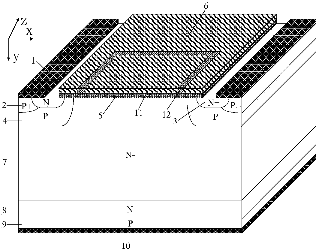
[0047] A planar gate IGBT, its semi-cellular structure and the section along the AB line are as follows image 3 and Figure 4 As shown, on the basis of Example 1, there is also an N-type layer 13 between the dielectric layer 5 and the N-drift region 7, and the doping concentration of the N-type layer 13 is equal to that of the N-drift region 7 10-100 times the doping concentration, the junction depth is 0.1-0.2 microns; and there is also a p-type buried layer 14 in the N-drift region 7 between the p-type base regions 4 in the lateral direction of the device, the The p-type buried layer 14 is 2-10 microns away from the p-type base region 4, and the p-type buried layer 14 is discontinuous and uniformly distributed in the N-drift region 7 in the longitudinal direction of the device, with a width of 1-5 microns and a spacing of 1-5 microns, the p-type buried layer 14 is in contact with the n-type layer 13 through the upper surface, and the junction depth of the p-type buried lay...

Embodiment 3

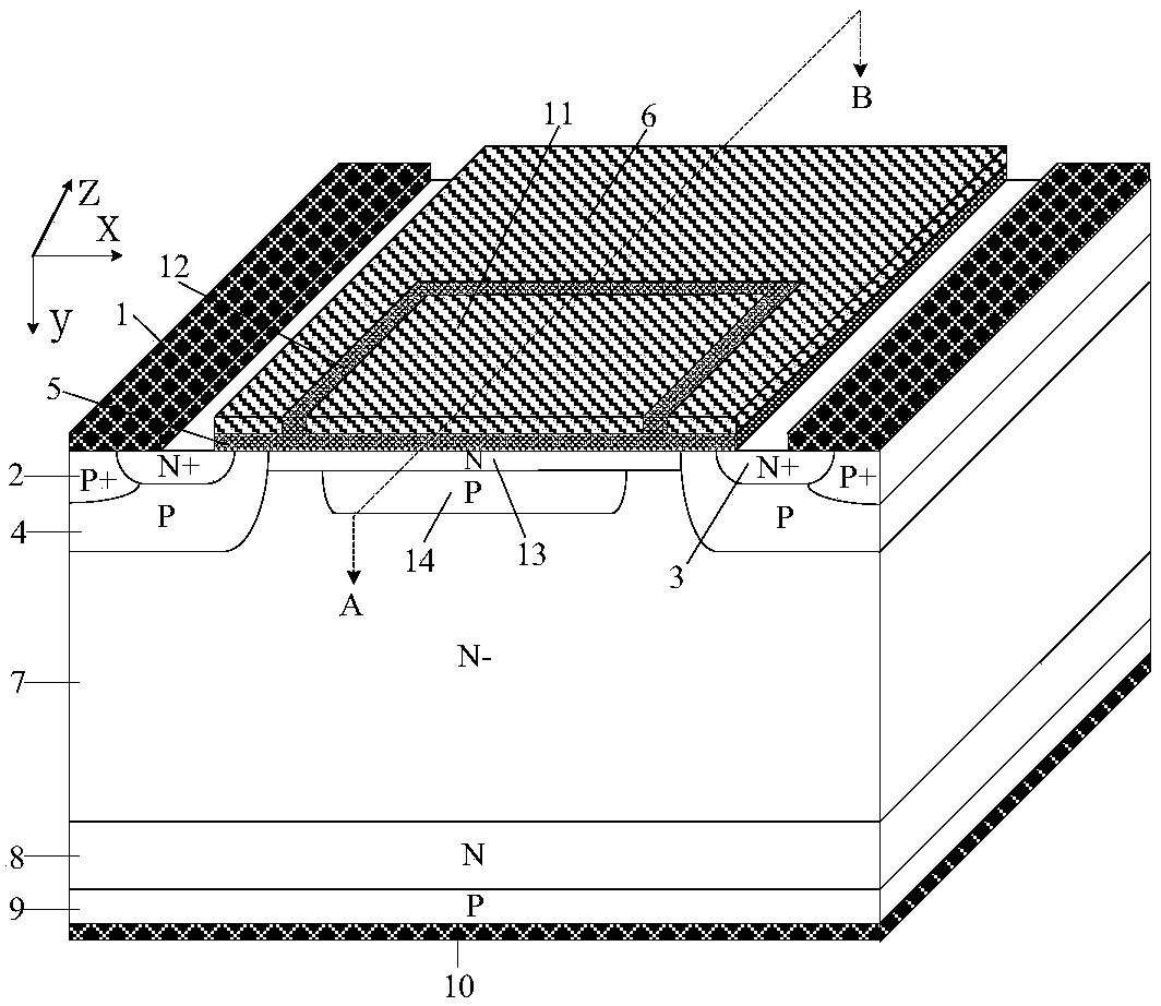
[0049] A planar gate IGBT, its semi-cellular structure and the section along the AB line are as follows Figure 5 and Figure 6As shown, on the basis of Example 2, there is also a layer of N in the N-drift region 7 between the p-type buried layer 14 and between both sides of the p-type buried layer 14 and the p-type base region 4 Type buried layer 15, the N-type buried layer 15 is in contact with the N-type layer 13 through the upper surface and its junction depth is 0.2-0.5 micron, the doping concentration of the N-type buried layer 15 is N-drift region 7 doped 10-100 times the impurity concentration. The introduction of the N-type buried layer 15 further improves the forward conduction characteristics of the device. When the device breaks down, the N-type buried layer 15 is fully depleted.


PUM


Abstract

The invention belongs to the technical field of power semiconductor devices, and relates to a planar gate IGBT and a manufacturing method thereof. On the basis of the traditional planar gate IGBT device structure, the present invention introduces an electrode connected to the emitter in the upper part of the oxide layer of the JFET region of the device, and the emitter connection electrode and the gate form a space in a direction perpendicular to the length of the MOS channel. Distribution, in the JFET region, through the lateral carrier diffusion from the gate to the emitter connection electrode in the direction perpendicular to the MOS channel length, the structure of the present invention reduces the device's forward conduction characteristics without affecting the device. The gate capacitance, especially the gate-collector capacitance, improves the switching speed of the device and reduces the switching loss of the device without degrading the blocking characteristics of the device.

Description

technical field [0001] The invention belongs to the technical field of power semiconductor devices, and relates to an insulated gate bipolar transistor (IGBT), in particular to a planar gate insulated gate bipolar transistor. Background technique [0002] Insulated Gate Bipolar Transistor (IGBT) is a new type of power electronic device combining MOS field effect and bipolar transistor. It not only has the advantages of easy driving and simple control of MOSFET, but also has the advantages of low conduction voltage of power transistor, large on-state current and small loss. It has become one of the core electronic components in modern power electronic circuits and is widely used in Various fields of the national economy such as communications, energy, transportation, industry, medicine, household appliances and aerospace. The application of IGBT plays an extremely important role in improving the performance of power electronic systems. [0003] Since the invention of IGBT, ...

Claims


Application Information

Patent Timeline
Patent Type & Authority Patents(China)
IPC IPC(8): H01L29/739H01L29/417H01L21/331H01L29/423
CPCH01L29/41708H01L29/42356H01L29/66333H01L29/7395
Inventor 张金平陈文梅黄孟意田丰境刘竞秀李泽宏任敏张波
Owner UNIV OF ELECTRONICS SCI & TECH OF CHINA
Why Eureka
Try Eureka