Flexible silicon-based nanometer thin film thermoelectric device

A nano-thin film and thermoelectric device technology, applied in the manufacture/processing of thermoelectric devices, thermoelectric device junction lead-out materials, thermoelectric devices that only use the Peltier or Seebeck effect, etc., can solve the problem of not being able to adapt to high-temperature annealing and difficult to silicon-based devices Integration, high cost and other issues, achieve the effect of reducing internal stress, good thermal conductivity, and improving thermoelectric performance

Active Publication Date: 2016-08-17
GUILIN UNIV OF ELECTRONIC TECH
View PDF8 Cites 9 Cited by
  • Summary
  • Abstract
  • Description
  • Claims
  • Application Information

AI Technical Summary

Problems solved by technology

The polymer material substrate cannot adapt to high-temperature annealing, reflow soldering and other processes in the process of device preparation, and there is a large Schottky contact resistance between gold, silver, copper electrode materials and thermoelectric arm materials, resulting in the flexible thermoelectric devices reported so far. There are disadvantages of low efficiency, high cost, and difficulty in integrating with silicon-based devices

Method used


Image

  • Flexible silicon-based nanometer thin film thermoelectric device
  • Flexible silicon-based nanometer thin film thermoelectric device
  • Flexible silicon-based nanometer thin film thermoelectric device

Examples


Embodiment 1

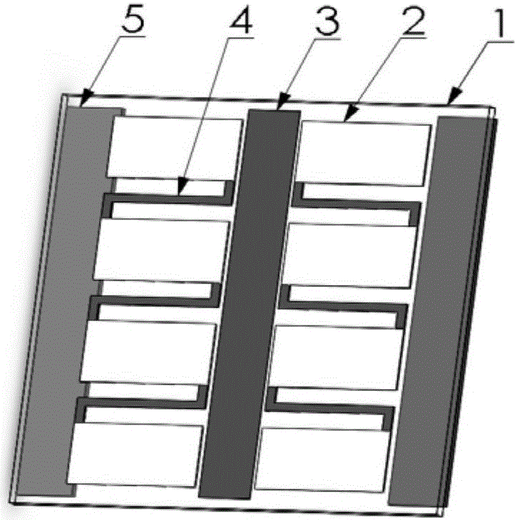
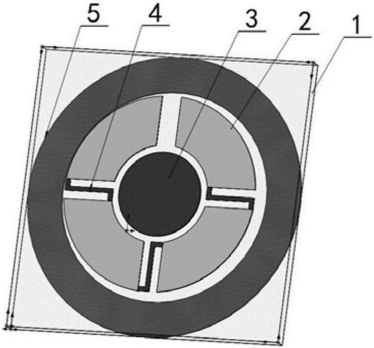
[0030] see Figure 1 to Figure 6 , a flexible silicon-based nano-thin film thermoelectric device, including a flexible glass substrate 1, on which a P-type silicon-based nano-thin film thermoelectric arm 2, a graphene electrode 4, a heat-end heat-absorbing graphene coating 5 and The graphene coating 3 for heat dissipation at the cold end, and the array of P-type silicon-based nano-film thermoelectric arms 2 are connected by graphene electrodes 4; The graphene coating 3 is disposed on the heat dissipation end surface of the flexible glass substrate 1 .

[0031] The P-type silicon-based nano-film thermoelectric arm 2 is prepared by magnetron sputtering. In the coating chamber, the background vacuum is 4.2×10 -4 Pa, after ignition and target washing for 10-15min, simultaneously turn on the Si target and Ge target for co-sputtering, and control the sputtering power of Si to 100W, and the sputtering power of Ge to 60W, and sputter for 6min. Then close the Si target and Ge target...

Embodiment 2

[0037] see Figure 1 to Figure 6 , a flexible silicon-based nano-thin film thermoelectric device, including a flexible glass substrate 1, on which a P-type silicon-based nano-thin film thermoelectric arm 2, a graphene electrode 4, a heat-end heat-absorbing graphene coating 5 and The graphene coating 3 for heat dissipation at the cold end, and the array of P-type silicon-based nano-film thermoelectric arms 2 are connected by graphene electrodes 4; The graphene coating 3 is disposed on the heat dissipation end surface of the flexible glass substrate 1 .

[0038] The P-type silicon-based nano-film thermoelectric arm 2 is prepared by magnetron sputtering. In the coating chamber, the background vacuum is 4.2×10 -4 Pa, after ignition and target washing for 10-15min, simultaneously turn on the Si target and Ge target for co-sputtering, and control the sputtering power of Si to 100W, and the sputtering power of Ge to 60W, and sputter for 6min. Then close the Si target and Ge target...


PUM

PropertyMeasurementUnit
electrical resistivityaaaaaaaaaa

Abstract

The invention proposes a flexible silicon-based nanometer thin film thermoelectric device. The flexible silicon-based nanometer thin film thermoelectric device comprises a flexible glass substrate, wherein silicon-based nanometer thin film thermoelectric arms, graphene electrodes and a graphene coating layer are arranged on the flexible glass substrate, the silicon-based nanometer thin film thermoelectric arms are deposited on the flexible glass substrate by a physical vapor deposition technology, and the silicon-based nanometer thin film thermoelectric arms are connected by the graphene electrodes. In the flexible silicon-based nanometer thin film thermoelectric device, the flexible glass substrate is adopted, a high-temperature rapid annealing process can be adopted during the preparation process of a nanometer silicon-based thin film deposited on the surface of the substrate, the generation of quantum dots and superlattices are facilitated, and the thermoelectric performance of the silicon-based nanometer thin film is substantially improved.

Description

Technical field: [0001] The invention relates to the field of thermoelectric technology, in particular to a flexible silicon-based nano-film thermoelectric device. Background technique: [0002] With the rapid increase of human demand for energy, non-renewable energy sources such as oil and natural gas have begun to be exhausted, and environmental pollution problems have emerged in the process of use. Therefore, the development and application of new energy materials and technologies have attracted much attention. Compared with renewable energy power generation systems such as solar energy and wind energy, the working medium of semiconductor thermoelectric devices is electrons conducted in solids, so it has no working medium leakage, no mechanical movement, no vibration and noise, long life, small size, It has the advantages of light weight, easy integration with other electronic and optoelectronic devices. [0003] Since 2013, with the rapid rise and rapid development of ...

Claims


Application Information

Patent Timeline
Patent Type & Authority Applications(China)
IPC IPC(8): H01L35/12H01L35/28H01L35/34H10N10/85H10N10/01H10N10/10
CPCH10N10/85H10N10/10H10N10/01
Inventor 彭英苗蕾王潇漾刘呈燕
Owner GUILIN UNIV OF ELECTRONIC TECH
Why Eureka
Try Eureka