TFT (thin film transistor) array substrate and manufacturing method therefor, and liquid crystal display apparatus

A technology for liquid crystal display devices and array substrates, which is applied in semiconductor/solid-state device manufacturing, instruments, semiconductor devices, etc., can solve the problems of large resistance values ​​of metals and semiconductors, reduce Schottky barriers, reduce distances, and improve The effect of electrical characteristics

Inactive Publication Date: 2016-08-24
TCL CHINA STAR OPTOELECTRONICS TECH CO LTD
View PDF3 Cites 13 Cited by
  • Summary
  • Abstract
  • Description
  • Claims
  • Application Information

AI Technical Summary

Problems solved by technology

But TFT devices require electrical contact, and this contact must be low resistance rather than rectifying
For this reason, it is often necessary to dope the semiconductor to make M2 and A-Si form an ohmic contact, but even if A-Si is doped with P, the resistance of the metal and the semiconductor is still very large

Method used


Image

  • TFT (thin film transistor) array substrate and manufacturing method therefor, and liquid crystal display apparatus
  • TFT (thin film transistor) array substrate and manufacturing method therefor, and liquid crystal display apparatus
  • TFT (thin film transistor) array substrate and manufacturing method therefor, and liquid crystal display apparatus

Examples


Embodiment Construction

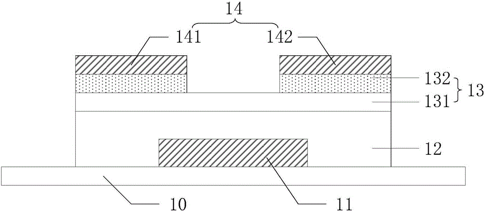
[0029] Refer to figure 1 , figure 1 It is a schematic structural view of an embodiment of the TFT array substrate of the present invention. The TFT array substrate includes a substrate 10 and a TFT disposed on the substrate 10.

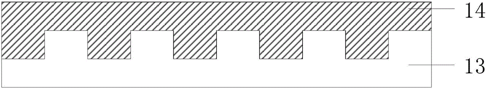
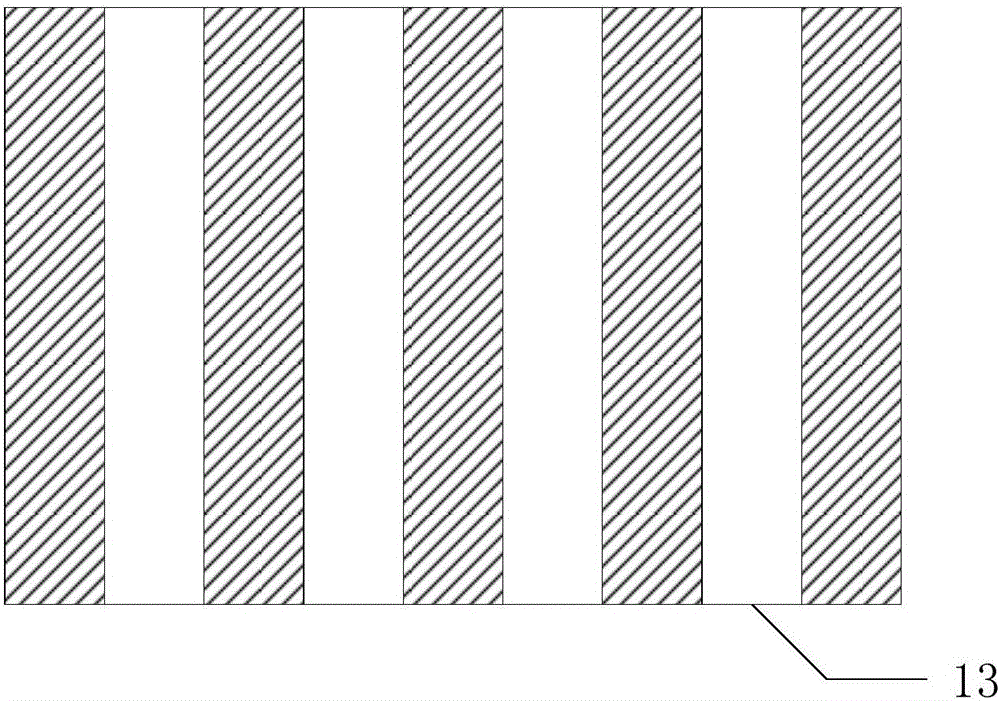
[0030] Wherein, the TFT includes a gate 11, a gate insulating layer 12, a semiconductor layer 13, and a source-drain layer 14 which are sequentially arranged on the substrate 10, wherein the source-drain layer 14 includes a source 141 and a drain 142.

[0031] Optionally, the substrate 10 may be a glass substrate or a plastic substrate.

[0032] Optionally, the gate 11 and the source drain layer 14 are metal layers.

[0033] Optionally, the gate insulating layer 12 may be SiO x Or SiN x , Can also be SiO x And SiN x The mixture can also include a layer of SiO x And a layer of SiN x .

[0034] Optionally, the semiconductor layer 13 may be one of amorphous silicon (A-Si), polysilicon (P-Si), or low temperature polysilicon (LTPS), or may be doped semiconductors of...


PUM


Abstract

The invention discloses a TFT (thin film transistor) array substrate and a manufacturing method therefor, and a liquid crystal display apparatus. The TFT array substrate comprises a substrate and the TFT arranged on the substrate; the TFT comprises a semiconductor layer and a source electrode and a drain electrode arranged on the semiconductor layer, wherein the contact surface between the semiconductor layer and the source electrode and / or the drain electrode adopts a concave-convex structure. By adoption of the mode, the contact resistance between the semiconductor layer and a metal layer can be lowered, so that the electrical property of the TFT device is improved.

Description

Technical field [0001] The present invention relates to the field of display technology, in particular to a TFT array substrate, a manufacturing method thereof, and a liquid crystal display device. Background technique [0002] TFT (Thin Film Transistor) is an abbreviation for thin film transistor. TFT means that each liquid crystal pixel on the liquid crystal display is driven by a thin film transistor integrated behind it, so that it can display screen information at high speed, high brightness and high contrast. TFT-LCD (thin film transistor liquid crystal display) is the majority A type of liquid crystal display. [0003] In the preparation process of TFT, the contact interface treatment between M2 (the metal layer where the source / drain is located) and A-Si (amorphous silicon) is a very important part, because there is a potential energy difference between metal and A-Si. Form Schottky contacts. But TFT devices require electrical contacts, and such contacts must be low resi...

Claims


Application Information

Patent Timeline
Patent Type & Authority Applications(China)
IPC IPC(8): H01L27/12H01L21/77G02F1/1368
CPCG02F1/1368H01L27/1222H01L27/127H01L29/66969H01L29/41733H01L29/78618H01L29/7869H01L29/78666H01L27/124H01L29/66765G02F2202/10G02F2202/103H01L27/1225H01L29/1604H01L29/24H01L29/78669H01L29/78696
Inventor 吕晓文
Owner TCL CHINA STAR OPTOELECTRONICS TECH CO LTD
Why Eureka
Try Eureka