TFT (Thin Film Transistor) and display device

一种薄膜晶体管、显示装置的技术,应用在晶体管、半导体器件、仪器等方向,能够解决影响液晶显示器显示效果、降低液晶显示器显示品质等问题,达到提高显示品质、减弱电容耦合效应、降低寄生电容的效果

Inactive Publication Date: 2016-08-24
TCL CHINA STAR OPTOELECTRONICS TECH CO LTD
View PDF4 Cites 10 Cited by
  • Summary
  • Abstract
  • Description
  • Claims
  • Application Information

AI Technical Summary

Problems solved by technology

The increased parasitic capacitance will lead to a greater degree of capacitive coupling effect and signal delay effect, which will affect the display effect of the liquid crystal display and reduce the display quality of the liquid crystal display

Method used


Image

  • TFT (Thin Film Transistor) and display device
  • TFT (Thin Film Transistor) and display device
  • TFT (Thin Film Transistor) and display device

Examples


Embodiment 1

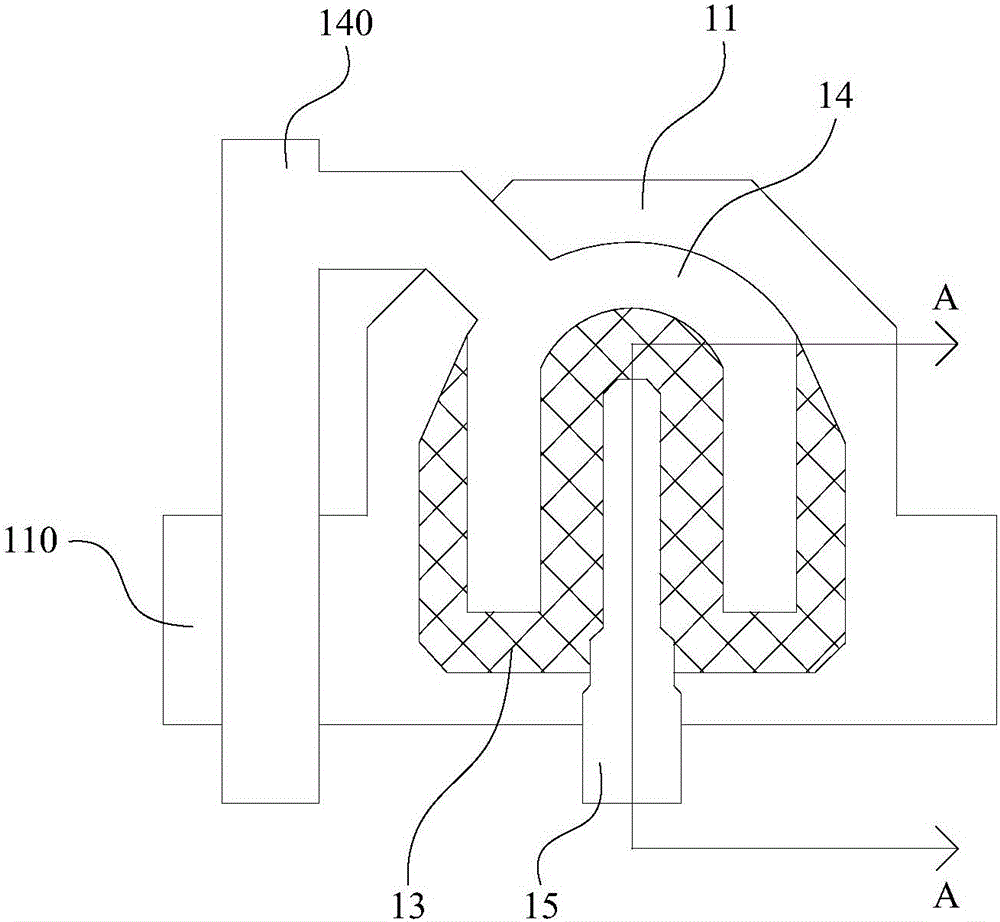
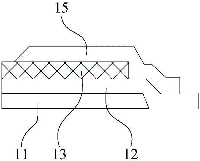
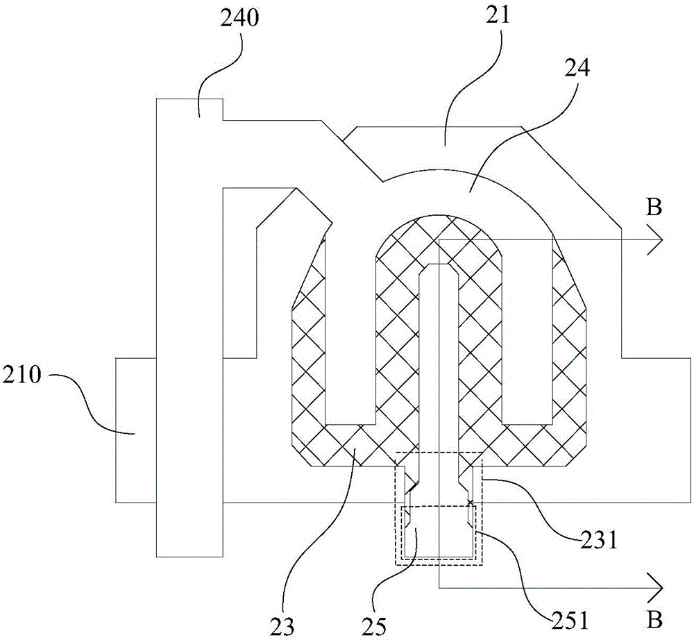
[0031] An embodiment of the present invention provides a thin film transistor, which can be applied to a liquid crystal display. Such as image 3 and Figure 4 As shown, this embodiment takes an amorphous silicon (a-Si) thin film transistor as an example for scanning. The thin film transistor includes a gate 21 from bottom to top, and a gate insulating layer covering the gate 21. 22 , a semiconductor layer 23 formed on the gate insulating layer 22 , and a source 24 and a drain 25 formed on the semiconductor layer 23 . Wherein, the gate electrode 21 is connected to the scan line 210 , and the source electrode 24 is connected to the data line 240 . The gate 21 and the scan line 210 are located on the first metal layer, and the source 24 , the drain 25 and the data line 240 are located on the second metal layer. The semiconductor layer 23 has an extension portion 231 , the plane projection of the extension portion 231 exceeds the edge of the gate 21 , and the drain 25 covers t...

Embodiment 2

[0042] An embodiment of the present invention provides a display device, which is preferably a high PPI (Pixels Per Inch) display device such as a mobile phone or a tablet computer, that is, a display device with a high number of pixels per inch. The PPI value of the display device in this embodiment is above 400.

[0043] The display device provided by the embodiment of the present invention includes an array substrate, a color filter substrate, and a liquid crystal layer filled between the array substrate and the color filter substrate. Wherein, sub-pixels arranged in an array are formed on the array substrate, and each sub-pixel is provided with the thin film transistor provided in the first embodiment above.


PUM


Abstract

The invention discloses a TFT (Thin Film Transistor) and a display device, belongs to the technical field of display and can reduce stray capacitance between a first metal layer and a second metal layer and increase the display quality of an LCD (Liquid Crystal Display). The TFT comprises a grid electrode, a grid electrode insulation layer, a semiconductor layer, a source electrode and a drain electrode, wherein the grid electrode insulation layer covers the grid electrode; the semiconductor layer is formed on the grid electrode insulation layer; the source electrode and the drain electrode are formed on the semiconductor layer; the semiconductor layer is provided with an extension part; a planar projection of the extension part exceeds the edge of the grid electrode, and the drain electrode covers the extension part. The TFT disclosed by the invention can be applied to high-PPI (Pixel Per Inch) display devices such as a mobile phone and a tablet computer.

Description

technical field [0001] The invention relates to the field of display technology, in particular to a thin film transistor and a display device. Background technique [0002] With the development of display technology, thin film transistor liquid crystal display (Thin Film Transistor Liquid Crystal Display, referred to as TFT-LCD) has become the most common display device. important display platform. [0003] The thin film transistors play a very important role in active matrix display technology. Specifically, in an active matrix liquid crystal display, each sub-pixel is configured with a thin film transistor, so that each sub-pixel can operate independently and is not easily affected by other sub-pixels. Such as figure 1 and figure 2 As shown, most of the current TFTs adopt a bottom-gate structure, which includes gate 11 , gate insulating layer 12 , semiconductor layer 13 , and source 14 and drain 15 on the same layer from bottom to top. Wherein, the gate electrode 11 ...

Claims


Application Information

Patent Timeline
Patent Type & Authority Applications(China)
IPC IPC(8): H01L29/786H01L29/08G02F1/1362
CPCG02F1/1362H01L29/0847H01L29/786H01L29/78618H01L29/41733G02F1/1368H01L29/08G02F1/13606H01L29/41775H01L29/78696
Inventor 雍玮娜
Owner TCL CHINA STAR OPTOELECTRONICS TECH CO LTD
Why Eureka
Try Eureka