Etching pattern overprinting high-precision alignment method and device
An alignment device, high-precision technology, applied in sustainable manufacturing/processing, electrical components, climate sustainability, etc., can solve the problem of low alignment accuracy between mask patterns and electrode patterns, and achieve mask cost savings, The effect of reducing production cost and reducing line width
- Summary
- Abstract
- Description
- Claims
- Application Information
AI Technical Summary
Problems solved by technology
Method used
Image
Examples
Embodiment 1
[0026] Such as Figure 1-6 As shown, a high-precision alignment method for etching pattern overprinting includes the following steps:
[0027] S1: Provide silicon wafer and slurry carrier;
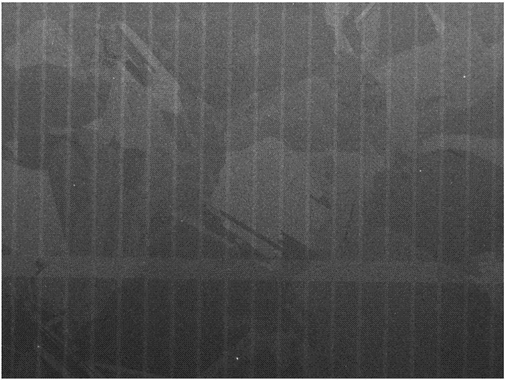
[0028] S2: The visual recognition system takes pictures of silicon wafers;
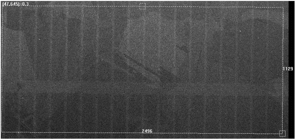
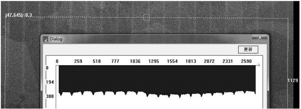
[0029] S3: Select a ROI area at a fixed position on the picture, and obtain a group of data in the ROI area through the vertical projection method, preprocess the data through the discrete data curve smoothing algorithm, and calculate the peak position and line width; image 3 , Figure 4 shown;
[0030] Due to the image acquisition process and the film itself, the data curve has noise points, the data is preprocessed by the discrete data curve smoothing algorithm, and then the position and line width of the wave peak can be calculated;
[0031] In this embodiment, a five-point quadratic filtering curve smoothing algorithm is used;
[0032] Taking the C language code as an example, the specific algorithm is a...
Embodiment 2
[0059] A high-precision alignment device for etching pattern overprinting, comprising:
[0060] A visual recognition device for taking and recording pictures of the silicon wafer surface; a motion device for rotating and moving the silicon wafer; and, for receiving and processing image information input by the visual recognition system and outputting control commands to the motion device and laser scanning device control system; the visual recognition device includes an industrial camera with the lens facing the silicon wafer, a light source that provides light for the camera, and an image acquisition component that collects images collected by the camera. The camera, image acquisition component, motion device and laser scanning device pass through the The communication transmission cable is connected to the control system. The laser scanning device is an etching device in the etching process, and is a component in the prior art.
[0061] Using the etching pattern overprintin...
PUM
 Abstract
Description
Claims
Application Information


