Film bulk acoustic resonator having multiple resonance modes and preparation method thereof and filter
A thin-film bulk acoustic wave and resonator technology, applied in electrical components, impedance networks, etc., can solve the problems of unfavorable RF front-end miniaturization, integrated development, increasing the complexity of the external impedance of the filter, and difficulty in debugging the whole machine. The whole machine is debugged, the difficulty of production is reduced, and the effect of integration is beneficial
- Summary
- Abstract
- Description
- Claims
- Application Information
AI Technical Summary
Problems solved by technology
Method used
Image

Examples
Embodiment 1
[0039] The thin film bulk acoustic resonator of the multi-resonance mode of this embodiment is prepared by the following preparation method:
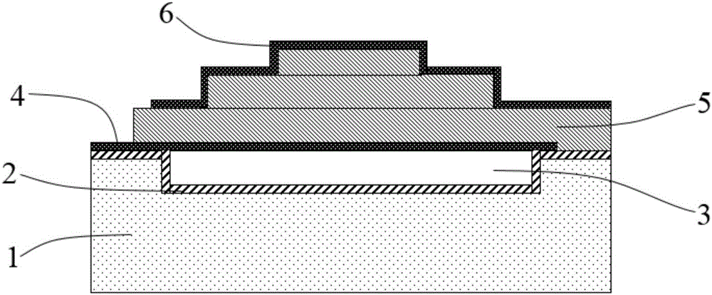
[0040] 1. Etch a groove on the surface of the silicon substrate 1 with a depth of 30 μm, and then deposit Si by PECVD 3 N 4 The substrate protection layer 2 has a thickness of 200nm to protect the silicon substrate. Such as figure 1 shown.
[0041] 2. In Si 3 N 4 A layer of PSG (phospho-quartz glass) is deposited on it by PECVD as a sacrificial layer.
[0042] 3. The surface of the sacrificial layer is polished by a CMP process.
[0043] 4. A layer of Mo bottom electrode 4 with a thickness of 200 nm is deposited on the polished surface by DC magnetron sputtering, and patterned by photolithography.
[0044] 5. Using radio frequency magnetron sputtering to deposit C-axis preferred orientation AlN piezoelectric film. And a multi-layer structure is etched by photolithography and ICP. This embodiment is a three-layer AlN piezoelectr...
Embodiment 2
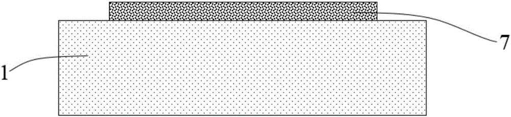
[0050] 1. A layer of PSG (phosphorus quartz glass) is deposited by PECVD on the surface of the silicon substrate 1 as the sacrificial layer 7, and a pattern of the sacrificial layer is photoetched. Such as image 3 shown.
[0051] 2. Deposit a layer of Si by PECVD 3 N 4 The supporting layer 8 has a thickness of 300nm.
[0052] 3. A layer of Mo bottom electrode 4 with a thickness of 150 nm is patterned by photolithography and magnetron sputtering.
[0053] 4. Using radio frequency magnetron sputtering to deposit C-axis preferred orientation AlN piezoelectric film. And a multi-layer structure is etched by photolithography and ICP. This embodiment is a three-layer AlN piezoelectric film, and the area size of the AlN piezoelectric film decreases successively from bottom to top; the thickness of each layer is 2 μm, 0.8 μm, and 0.5 μm from bottom to top.
[0054] 5. A layer of Mo top electrode 6 with a thickness of 150 nm is patterned by photolithography and electron beam evap...
PUM
| Property | Measurement | Unit |
|---|---|---|
| Thickness | aaaaa | aaaaa |
| Thickness | aaaaa | aaaaa |
| Thickness | aaaaa | aaaaa |
Abstract
Description
Claims
Application Information
 - R&D
- Intellectual Property
- Life Sciences
- Materials
- Tech Scout
- Unparalleled Data Quality
- Higher Quality Content
- 60% Fewer Hallucinations
Browse by: Latest US Patents, China's latest patents, Technical Efficacy Thesaurus, Application Domain, Technology Topic, Popular Technical Reports.
© 2025 PatSnap. All rights reserved.Legal|Privacy policy|Modern Slavery Act Transparency Statement|Sitemap|About US| Contact US: help@patsnap.com