Power semiconductor device internal contact thermal resistance measurement method and measurement clamp

A technology of power semiconductor and measurement method, which is applied in the direction of single semiconductor device testing, measurement of electrical variables, measurement of electricity, etc., can solve the problems of difficulty in meeting the requirements of roughness and actual working conditions, destroying the phase relationship, and difficulty in guaranteeing

Inactive Publication Date: 2016-08-31
GLOBAL ENERGY INTERCONNECTION RES INST CO LTD +2
View PDF14 Cites 24 Cited by
  • Summary
  • Abstract
  • Description
  • Claims
  • Application Information

AI Technical Summary

Problems solved by technology

Conventional contact thermal resistance measurement methods include steady-state method and transient method. In the typical steady-state method, the temperature difference data of the contact surface is linearly extrapolated to obtain the contact thermal resistance. The data is reliable when it is large, and it is very difficult to accurately measure the temperature difference between the semiconductor device and the contact surface
The most widely used photothermal method in the transient method is to obtain the contact thermal resistance by measuring the phase difference (attenuation of wave amplitude) between the thermal wave (deformation wave) and the modulating wave after encountering the interface. The diffusion that causes the thermal wave to occur at the contact destroys its phase relationship, skewing the measurement
[0005] There are a large number of internal components of the press-fit IGBT device, and each component has a large area and thin thickness. It is not feasible to measure the temp

Method used


Image

  • Power semiconductor device internal contact thermal resistance measurement method and measurement clamp
  • Power semiconductor device internal contact thermal resistance measurement method and measurement clamp
  • Power semiconductor device internal contact thermal resistance measurement method and measurement clamp

Examples


Embodiment Construction

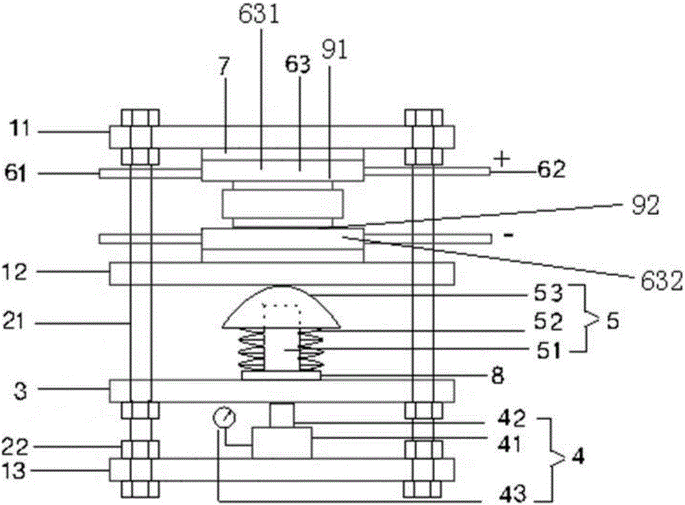
[0067] In order to describe the measurement scheme in the technical scheme provided by the present invention in more detail, it will be further described below in conjunction with the accompanying drawings and specific implementations.

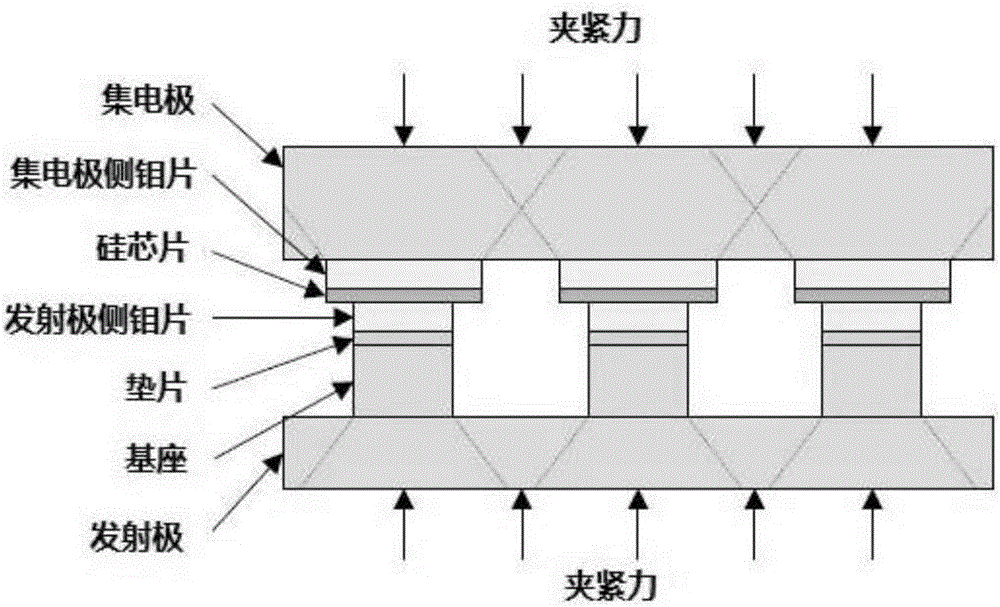
[0068] The structural schematic diagram of the existing IGBT crimping device is as follows: figure 1 As shown, it includes the collector, the molybdenum sheet on the collector side, the silicon chip, the molybdenum sheet on the emitter side, the spacer, the base, and the emitter in sequence. The number of internal components contained is large, and the area is relatively large and the thickness of each device is thin. , is mm level, in order to ensure the accurate measurement of the internal thermal contact resistance of the IGBT crimping device without damaging the integrity and excellent performance of the device, the present invention uses a measuring fixture to measure the internal thermal contact resistance to ensure that the devices are a...


PUM


Abstract

The invention provides a power semiconductor device internal contact thermal resistance measurement method and measurement clamp. The measurement method comprises the steps that a relation curve of device electrical parameters and junction temperature is drawn; a transient thermal impedance curve when liquid metal is coated between the surface of a device shell and a heat radiator is drawn; numeric calculation is performed on the transient thermal impedance curve so that the integral structure function and the differential structure function of the device are obtained; and a contact thermal resistance value is solved through reference to the integral structure function and the differential structure function. The measurement clamp is composed of three substrates arranged in a horizontal direction and two columns arranged in a vertical direction. An insulated plate and a heat radiation substrate are longitudinally and symmetrically arranged between the upper substrate and the intermediate substrate. A pressure uniform distribution device, a sensor, a pressure maintaining plate and a pressure applying device are installed between the intermediate substrate and the lower substrate in turn. According to the measurement method, measurement error caused by a thermocouple can be eliminated, the measurement result is real and reliable and the measurement method is simple and efficient.

Description

technical field [0001] The invention relates to the field of thermal resistance measurement of power semiconductor devices, in particular to a method for measuring internal contact thermal resistance of power semiconductor devices and a test fixture thereof. Background technique [0002] Compression-type power semiconductor devices such as transistors, IGBTs, IGCTs, and GTOs have been gradually applied to high-voltage direct current transmission (HVDC) in power systems due to their advantages such as high power density, double-sided heat dissipation, easy series connection, and high reliability. , electric locomotives and other high-voltage, high-power applications. [0003] Thermal resistance, which is an important standard for measuring the heat dissipation performance of semiconductor devices, is the most important parameter of semiconductor devices. The thermal resistance value of a device reflects the increase in power density and compact structure of semiconductor devi...

Claims


Application Information

Patent Timeline
IPC IPC(8): G01R31/26G01R1/04
CPCG01R1/0425G01R31/2601
Inventor 邓二平张朋赵志斌黄永章
Owner GLOBAL ENERGY INTERCONNECTION RES INST CO LTD
Why Eureka
Try Eureka