CMOS image sensor chip scale packaging method

An image sensor and chip-level packaging technology, applied in the field of image sensors, can solve the problems of complex process, high process cost, poor heat dissipation performance, etc., and achieve the effects of good heat dissipation performance, low process cost, and high process yield.

Active Publication Date: 2016-08-31
GALAXYCORE SHANGHAI
View PDF5 Cites 3 Cited by
  • Summary
  • Abstract
  • Description
  • Claims
  • Application Information

AI Technical Summary

Problems solved by technology

[0004] 1. The existing image sensor packaging method needs to fabricate the back-side lead-out structure on the image sensor, that is, the back-side lead-out structure cannot be separated from the image sensor and must be fabricated separately first, so the yield rate of the back-side lead-out structure is not easy to control independently, and the back-side lead-out structure cannot be separated from the image sensor. The manufacturing yield of the structure is not high, resulting in low packaging process yield;
[0005] 2. In addition to setting the rear lead-out structure in the existing image sensor packaging method, it is also necessary to set a protective substrate on the functional surface of the image sensor for protection. In this way, the functional surface and the back of the image sensor need to be increased to a certain thickness, so the image sensor cannot be integrated. The packaging structure is made thinner;
[0006] 3. When setting th

Method used


Image

  • CMOS image sensor chip scale packaging method
  • CMOS image sensor chip scale packaging method
  • CMOS image sensor chip scale packaging method

Examples


Embodiment Construction

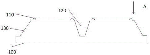
[0037] The invention provides a wafer-level packaging method of a CMOS image sensor, comprising: providing a wafer, the wafer has a plurality of image sensor chips, the image sensor chips have dicing lines between each other, and each of the image sensors The sensor chip has a photosensitive area and a non-photosensitive area, the photosensitive area has a pixel unit, and the non-photosensitive area has a first electrode; a support frame is provided, and the support frame is fixed on the image sensor chip, and the support The inner opening of the frame exposes the photosensitive area, the support frame does not completely cover the first electrode, a conductive layer is formed on the surface of the first electrode and the support frame, and is electrically connected to the top contact of the support frame; along the cutting road The wafer is diced to form packages.

[0038] In order to make the above objects, features and advantages of the present invention more comprehensible...


PUM

PropertyMeasurementUnit
Widthaaaaaaaaaa
Lengthaaaaaaaaaa

Abstract

The invention provides a CMOS image sensor wafer scale packaging method comprising the steps that a wafer is provided, the wafer is provided with multiple image sensor chips, cutting channels are arranged between the image sensor chips, each image sensor chip is provided with a light-sensitive area and a non-light-sensitive area, the light-sensitive area is provided with pixel units, and the non-light-sensitive area is provided with first electrodes; a supporting frame is provided, the supporting frame is fixed on the image sensor chips, the internal side of the supporting frame is open and the light-sensitive area is exposed, the supporting frame does not completely cover the first electrodes, a conductive layer is formed on the surface of the first electrodes and the supporting frame and electrically connected with the top contacts of the supporting frame; and the wafer is cut along the cutting channels so as to form packaging members.

Description

technical field [0001] The invention relates to the field of image sensors, and is characterized in that it relates to a chip-level packaging method of a CMOS image sensor. Background technique [0002] An image sensor is a semiconductor device device that converts optical information into electrical signals. Existing image sensors can be further classified into complementary metal oxide semiconductor (CMOS) image sensors and charge coupled device (CCD) image sensors. [0003] Image sensors are developing toward miniaturization, and the new generation of electronic products has higher requirements for image sensor packaging structures, such as smaller shape and lower cost. However, traditional image sensor packaging methods usually lead the pads on the functional surface of the image sensor to the back, and then make conductive solder balls or pins on the back, so that the obtained image sensor packaging structure can be connected to external circuits. However, the existin...

Claims


Application Information

Patent Timeline
IPC IPC(8): H01L27/146H01L27/148
CPCH01L27/14618H01L27/14636H01L27/14687H01L27/14689H01L27/14806
Inventor 赵立新邓辉
Owner GALAXYCORE SHANGHAI
Why Eureka
Try Eureka