Vertical structure AlGaInP-based light-emitting diode and manufacturing method thereof

A light-emitting diode and vertical structure technology, which is applied to electrical components, circuits, semiconductor devices, etc., can solve the problems of high production cost, numerous production steps, and low yield rate, and achieve the effect of simple manufacturing method and high product quality rate

Inactive Publication Date: 2016-09-07
YANGZHOU CHANGELIGHT
View PDF9 Cites 4 Cited by
  • Summary
  • Abstract
  • Description
  • Claims
  • Application Information

AI Technical Summary

Problems solved by technology

However, due to the many production steps and the very complic

Method used


Image

  • Vertical structure AlGaInP-based light-emitting diode and manufacturing method thereof

Examples


Embodiment Construction

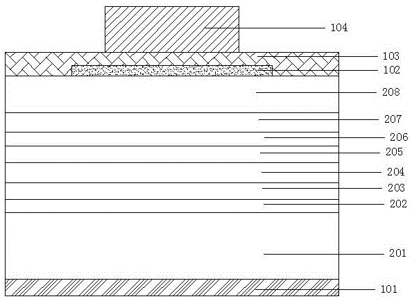
[0024] like figure 1 Shown:

[0025] 1. Manufacturing process:

[0026] 1. Making epitaxial wafers: using MOCVD equipment to sequentially grow N-GaAs buffer layer 202, AlAs / AlGaAs reflective layer 203, N-AlGaInP lower confinement layer 204, MQW multiple quantum well active Layer 205, P-AlGaInP upper confinement layer 206, P-GaInP buffer layer 207, P-GaP current spreading layer 208 doped with magnesium.

[0027] Among them, the P-GaP current spreading layer 208 preferably has a thickness of 4000 nm, and the doping elements are all magnesium (Mg), and the doping concentration is 2×10 19 cm -3 , to ensure a certain current expansion capability.

[0028] 2. Use No. 215 and No. 511 cleaning solutions to clean the P-GaP current spreading layer 208, and deposit SiO with a thickness of 100-350 nm on it by PECVD 2 , SiNx, TiO or TiO 2 Any one of them can be spin-coated with a positive photoresist, exposed and developed to produce a specific pattern. After plasma bonding, BOE was...


PUM

PropertyMeasurementUnit
Thicknessaaaaaaaaaa
Thicknessaaaaaaaaaa

Abstract

The invention provides a vertical structure AlGaInP-based light-emitting diode and a manufacturing method thereof, and belongs to the technical field of photoelectrons. The vertical structure AlGaInP-based light-emitting diode sequentially comprises a first electrode, a substrate, a semiconductor light-emitting layer, a current blocking layer, a transparent conductive layer and a second electrode from bottom to top, wherein the current blocking layer is arranged between the transparent conductive layer at the lower part of the second electrode and the semiconductor light-emitting layer; a current is injected into an indium tin oxide transparent thin film through the second electrode and is subjected to horizontal expansion on the transparent conductive layer due to the influence of the current blocking layer; and most of current is injected into an active region of the semiconductor light-emitting layer. By the distributed current injection method, accumulation of the current at the lower part of the electrode is slowed down; invalid injection of the current is reduced; and the light-emitting efficiency is improved.

Description

technical field [0001] The invention belongs to the technical field of optoelectronics, in particular to the technical field of manufacturing AlGaInP quaternary light-emitting diodes. Background technique [0002] Quaternary AlGaInP is a semiconductor material with direct wide bandgap, which has been widely used in the preparation of various optoelectronic devices. Since the light-emitting band of the material can cover the red to yellow-green band of visible light, the visible light-emitting diodes made therefrom have attracted extensive attention. [0003] The traditional vertical structure AlGaInP light-emitting diode uses a thick P-GaP current spreading layer to expand laterally and inject current into the light-emitting area. On the one hand, due to the limited current spreading ability of P-GaP, the current density in the vicinity of the electrode is relatively high, and the electrode is far away. The low current density in the area leads to low overall current inject...

Claims


Application Information

Patent Timeline
IPC IPC(8): H01L33/14H01L33/00
CPCH01L33/145H01L33/0062
Inventor 李波杨凯何胜徐洲林鸿亮张永张双翔
Owner YANGZHOU CHANGELIGHT
Why Eureka
Try Eureka