Silicon carbide bipolar junction transistor

A bipolar junction and transistor technology, applied to transistors, semiconductor devices, electrical components, etc., to reduce surface recombination current and increase current gain

Active Publication Date: 2016-09-21
INST OF MICROELECTRONICS CHINESE ACAD OF SCI
View PDF7 Cites 8 Cited by
  • Summary
  • Abstract
  • Description
  • Claims
  • Application Information

AI Technical Summary

Problems solved by technology

Although this structure reduces the recombination current and improves the current gain, it still does not fundamentally solve the problem of SiC / SiO 2 problems with high interface states; and SiO 2 The metal on the dielectric layer is an electrode that needs to be applied with a voltage, so the device with this structure is a four-terminal device. It is well known in the art that for triodes, four-terminal devices have many disadvantages compared with three-terminal devices

Method used


Image

  • Silicon carbide bipolar junction transistor
  • Silicon carbide bipolar junction transistor
  • Silicon carbide bipolar junction transistor

Examples


Embodiment Construction

[0020] In order to make the object, technical solution and advantages of the present invention clearer, the present invention will be further described in detail below in conjunction with specific embodiments and with reference to the accompanying drawings.

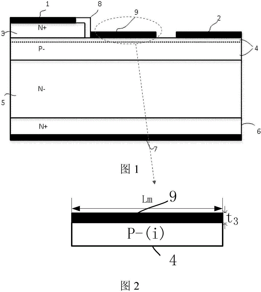
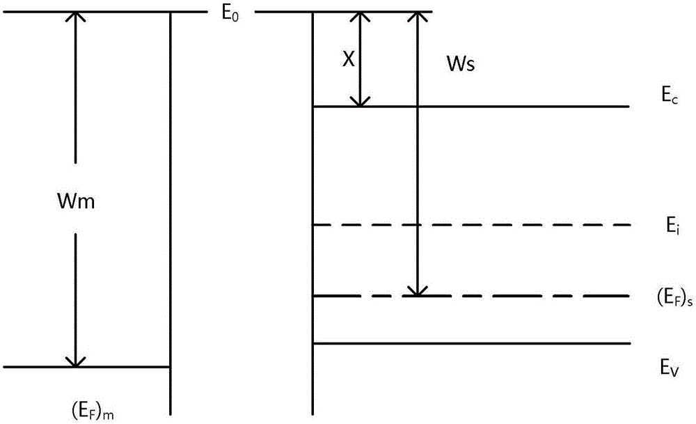
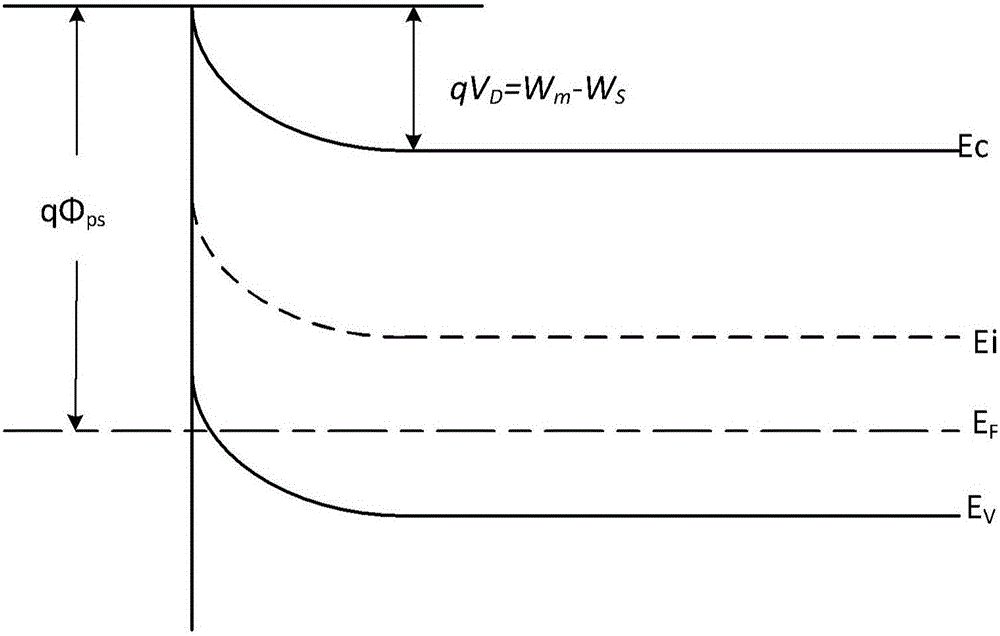
[0021] The invention discloses a silicon carbide bipolar junction transistor with a Schottky contact structure, which does not require an additional bias voltage electrode, and still maintains the device as a three-terminal device; and effectively solves the problem of SiC / SiO 2 The problem of high interface states improves the current gain of SiC BJT devices. More specifically, the present invention makes a Schottky contact structure on the surface of the outer base region between the edge of the emitter mesa and the base ohmic contact of the triode, and forms a Schottky barrier on the surface of the outer base region to prevent electrons Moving toward the surface, suppressing surface recombination and increasing the cur...


PUM


Abstract

The invention provides a silicon carbide bipolar junction transistor. The transistor is provided with a Schottky contact structure on an outer base area surface between a countertop edge of an emitter (1) and ohmic contact of a base (2), so as to form a Schottky barrier on the outer base area surface. The Schottky contact structure comprises a base area and a metal layer located on the base area. The silicon carbide bipolar junction transistor provided by the invention can prevent electrons from moving toward the surface through the Schottky contact structure, restrain the surface recombination and improve the current gain of the device.

Description

technical field [0001] The invention relates to the field of high-power semiconductor devices, in particular to a silicon carbide (SiC) bipolar junction transistor (BJT). Background technique [0002] The wide bandgap semiconductor material SiC is an ideal material for preparing high-voltage power electronic devices. Silicon carbide (SiC) bipolar junction transistor (BJT) is one of the important normally-off devices. Advantages. Compared with Si-based transistors, SiC BJT has the advantages of lower turn-on voltage and no secondary breakdown phenomenon; SiC BJT avoids the gate drive problem of normally-on device SiC JFET, and does not have the disadvantage of large conduction loss of SiC IGBT , there is no problem that the working conditions of the SiC MOSFET are limited due to the poor stability of the gate dielectric and the low mobility of the channel. [0003] SiC / SiO 2 The existence of high interface states will lead to adverse effects such as unstable gate dielectri...

Claims


Application Information

Patent Timeline
Patent Type & Authority Applications(China)
IPC IPC(8): H01L29/73H01L29/161H01L29/47
CPCH01L29/1608H01L29/47H01L29/73H01L29/7308
Inventor 郭飞申华军汤益丹张有润白云杨成樾宋凌云柏思宇彭朝阳
Owner INST OF MICROELECTRONICS CHINESE ACAD OF SCI
Why Eureka
Try Eureka