High-penetration-rate semiconductor bare chip manual eutectic welding method

A technology of eutectic welding and penetration rate, applied in semiconductor devices, semiconductor/solid-state device manufacturing, welding equipment, etc. Improve production efficiency and process applicability, low cost effect

Active Publication Date: 2016-09-28
BEIJING HUAHANG RADIO MEASUREMENT & RES INST
View PDF4 Cites 9 Cited by
  • Summary
  • Abstract
  • Description
  • Claims
  • Application Information

AI Technical Summary

Problems solved by technology

[0004] At present, in order to ensure a high eutectic penetration rate, vacuum sintering is often used for eutectic chips in large quantities. Using this method, special positioning and clamping tools must be prepared for each single chip, and must rely on Vacuum sintering furnace is an expensive equipment to realize assembly and welding, and the cost of process implementation is very high, and it is impossible to guarantee high production efficiency when implementing the application of small-batch and multi-variety research and development products.

Method used


Image

  • High-penetration-rate semiconductor bare chip manual eutectic welding method
  • High-penetration-rate semiconductor bare chip manual eutectic welding method

Examples


Embodiment Construction

[0024] The technical solution of the present invention will be described in detail below in conjunction with the accompanying drawings and specific embodiments.

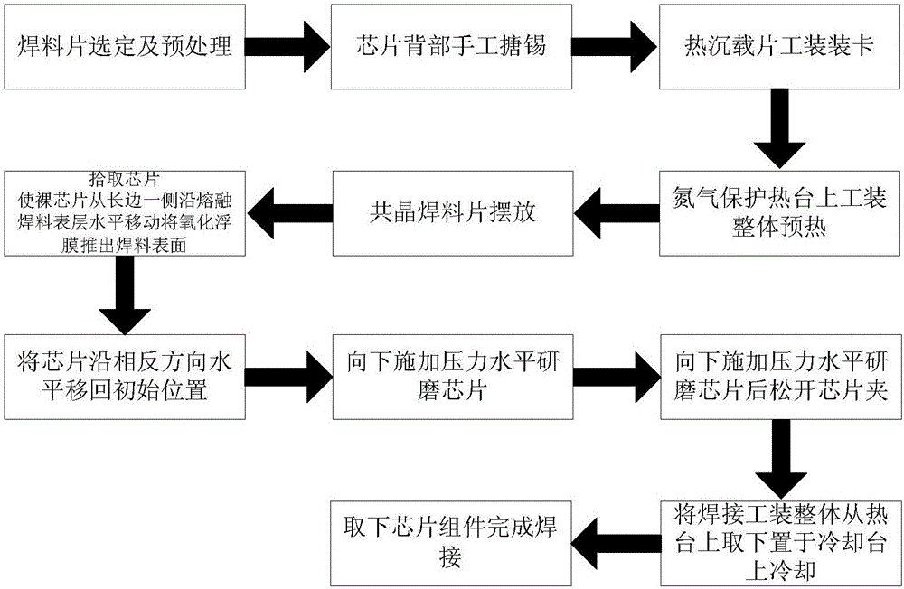
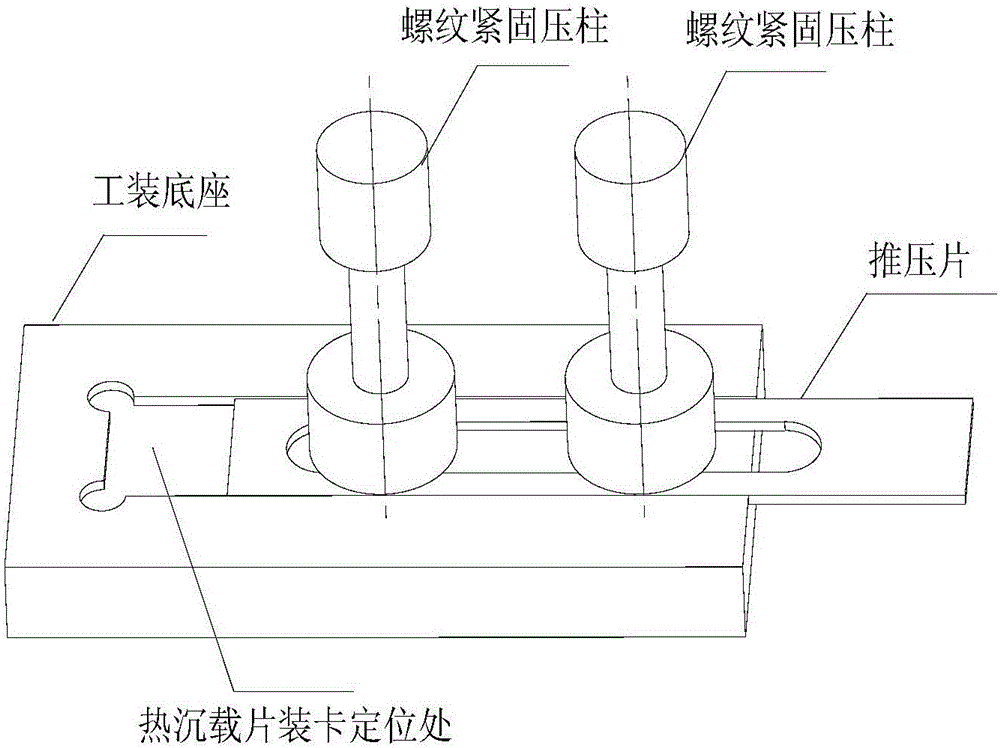
[0025] The technical process of the present invention based on pure manual high penetration rate eutectic welding method is as attached figure 1 shown.

[0026] Analyze the characteristics and application occasions of the bare chip to be soldered, select an alloy solder sheet with a suitable composition, and determine the size and thickness of the solder sheet according to the actual size of the chip.

[0027] According to the different uses of tinning and eutectic soldering on the back of the chip, the alloy solder sheet is reduced and cut according to the approximate shape of the chip (the size of the soldering sheet for tinning is 70% to 80% of the chip area, and the size of the eutectic soldering sheet is the chip area 85% to 90% of that).

[0028] The oxide film produced by long-term placement of chips and sol...


PUM

PropertyMeasurementUnit
thicknessaaaaaaaaaa

Abstract

The invention relates to a high-penetration-rate semiconductor bare chip eutectic welding method based on manual operation. According to the method, the penetration rate of semiconductor bare chip manual eutectic welding is greatly improved and the production efficiency and technology applicability can be effectively improved by arranging a reasonable and effective manual eutectic welding processes, and designing and using a general positioning clamping tool. The method is applicable to smalllot and diversified development-type products, and can effectively reduce the production cost and improve the production efficiency while ensuring the high welding quality.

Description

technical field [0001] The invention belongs to the field of packaging of electronic components, and in particular relates to a manual operation-based eutectic welding method for semiconductor bare chips with high penetration rate. Background technique [0002] With its small size, light weight, excellent high-frequency characteristics and high reliability, MMIC has been widely used in military satellite communications, phased array radar, navigation and other important fields. Microwave circuits usually have a high frequency (above 1GHz), so the grounding condition of the chip affects the circuit crosstalk and insertion loss, and also brings additional capacitance and oscillation. At the same time, the base material of the high-power MMIC chip used in the transmitting part of the T / R component has poor thermal conductivity, so the connection between the high-power chip and the base (substrate) must have very good microwave grounding capability (low ohm contact) and better h...

Claims


Application Information

Patent Timeline
Patent Type & Authority Applications(China)
IPC IPC(8): H01L21/60B23K1/00B23K1/20
CPCB23K1/00B23K1/20H01L24/03H01L24/09H01L24/80H01L2224/031
Inventor 王曦狄隽袁关东查家宏
Owner BEIJING HUAHANG RADIO MEASUREMENT & RES INST
Why Eureka
Try Eureka