Supercharge Your Innovation With Domain-Expert AI Agents!

Silicon carbide power device terminal structure and manufacturing method thereof

A technology of power device and terminal structure, which is applied in semiconductor/solid-state device manufacturing, semiconductor devices, electrical components, etc., to achieve the effects of reducing sensitivity, saving chip area, and shortening terminal length

Active Publication Date: 2016-09-28
杰平方半导体(上海)有限公司
View PDF6 Cites 10 Cited by
  • Summary
  • Abstract
  • Description
  • Claims
  • Application Information

AI Technical Summary

Problems solved by technology

Traditional silicon devices are limited by the characteristics of the material itself, getting closer and closer to its theoretical limit

Method used


Image

  • Silicon carbide power device terminal structure and manufacturing method thereof
  • Silicon carbide power device terminal structure and manufacturing method thereof
  • Silicon carbide power device terminal structure and manufacturing method thereof

Examples


Embodiment Construction

[0039] Embodiments of the present invention are described below through specific examples, and those skilled in the art can easily understand other advantages and effects of the present invention from the content disclosed in this specification. The present invention can also be implemented or applied through other different specific implementation modes, and various modifications or changes can be made to the details in this specification based on different viewpoints and applications without departing from the spirit of the present invention.

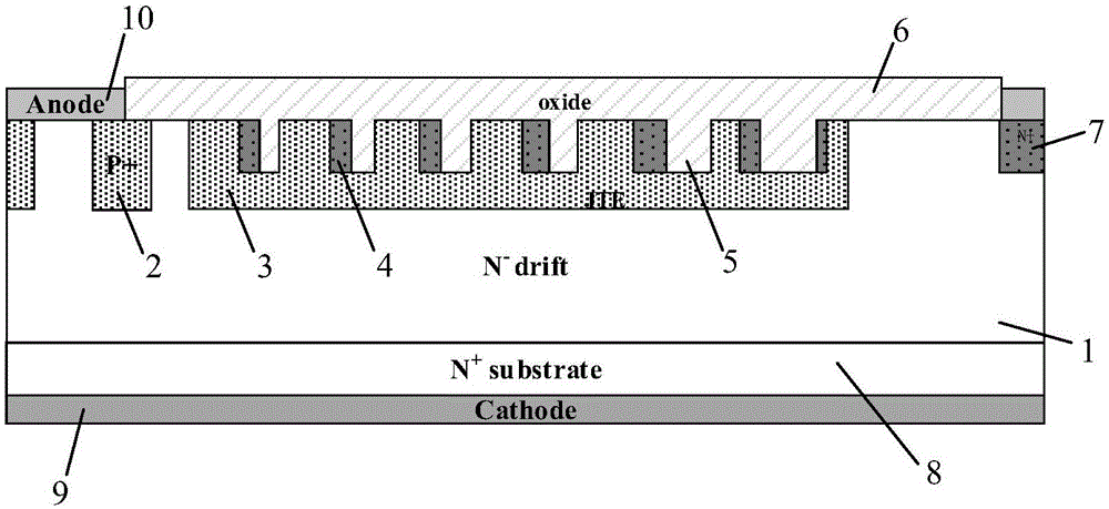
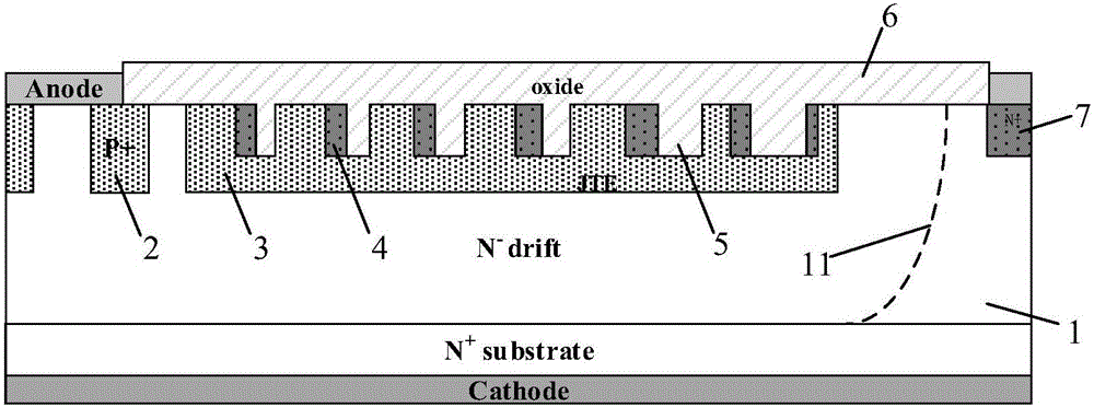
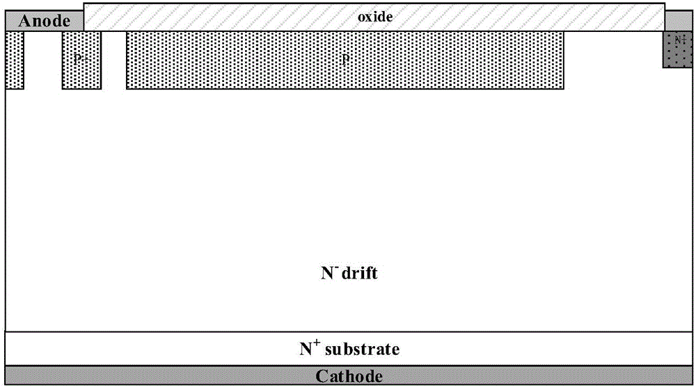
[0040] A silicon carbide power device terminal structure, including device cells and device terminals;

[0041] The device cell is a traditional junction barrier controlled Schottky structure, that is, there are several alternate heavily doped P-type body regions 2 connected to the anode metal 10 on the N-drift region 1;

[0042]The device terminal is located in the N-drift region 1 on the N-type heavily doped substrate 8, including t...


PUM


Abstract

The invention provides a silicon carbide power device terminal structure and a manufacturing method thereof. The silicon carbide power device terminal structure comprises a device cellular and a device terminal. The device terminal comprises a P-type junction terminal expansion region. The P-type junction terminal expansion region has N+ injection rings and etching grooves; the etching grooves are connected with the N+ injection rings, and the etching grooves are arranged at the outer sides of the N+ injection rings respectively; each etching groove is internally filled by an oxide layer; the adjacent N+ injection rings are separated by the etching grooves and the P-type junction terminal expansion region; the adjacent etching grooves are separated by the P-type junction terminal expansion region and the N+ injection rings; and the upper surface of the P-type junction terminal expansion region and the upper surfaces of the N+ injection rings are covered by the oxide layers. The silicon carbide power device terminal structure enables electric field distribution to be gentle, and enables a depletion layer of the terminal region to be fully expanded, thereby improving voltage withstand capability of the terminal, and reducing sensitivity degree of device breakdown voltage to the JTE region concentration. The structure can reduce partial electric field on the surface of the device, and meanwhile, reduces collision ionization rate of the surface of the device, thereby reducing surface electric leakage and improving reliability of the device surface.

Description

technical field [0001] The invention belongs to the technical field of semiconductor power devices. In particular, a silicon carbide power device terminal structure and a manufacturing method thereof. Background technique [0002] With the development of modern technology and the improvement of people's living standards, people continue to put forward higher requirements for semiconductor power devices in terms of volume, reliability, withstand voltage, and power consumption. Traditional silicon devices are limited by the characteristics of the material itself, getting closer and closer to its theoretical limit. In this context, people began to explore new materials other than silicon materials, and silicon carbide technology was born. Silicon carbide has a series of advantages that traditional silicon materials do not have, such as higher breakdown electric field, higher thermal conductivity, and larger forbidden band width, making silicon carbide more suitable for high-v...

Claims


Application Information

Patent Timeline
IPC IPC(8): H01L29/872H01L29/06H01L21/329
CPCH01L29/0619H01L29/6606H01L29/872
Inventor 邓小川柏思宇宋凌云陈茜茜张波
Owner 杰平方半导体(上海)有限公司
Features
  • R&D
  • Intellectual Property
  • Life Sciences
  • Materials
  • Tech Scout
  • Unparalleled Data Quality
  • Higher Quality Content
  • 60% Fewer Hallucinations
Learn More