A kind of device and method for preparing amorphous carbon and nitrogen film on silicon surface
An amorphous carbon nitrogen and silicon surface technology, applied in vacuum evaporation plating, coating, sputtering plating, etc., can solve the problems of system research, effective control of content and distribution, etc., and achieve uniform structure distribution and chemical bond content And the effect of controllable structure and uniform distribution
- Summary
- Abstract
- Description
- Claims
- Application Information
AI Technical Summary
Problems solved by technology
Method used
Image
Examples
Embodiment 1
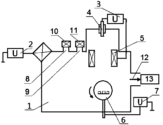
[0039] use figure 1 The shown device prepares atomized nitrogen-doped amorphous carbon-nitride film on the surface of silicon substrate.
[0040] A single crystal silicon substrate with a diameter of 20 mm and a thickness of 0.5 mm was tested, and the operation steps were as follows:
[0041] (1) Surface treatment of silicon substrate: Place the monocrystalline silicon wafer into acetone solution, ethanol solution and deionized water for 10 minutes to ultrasonically clean each to remove surface grease and other pollutants, then place the substrate in an oven to dry for use ;
[0042] (2) Fix the pretreated silicon substrate on such as figure 1 On the rotating sample stage in the vacuum chamber of the cathodic arc device shown, the high-purity graphite target is used as the cathode of the pulsed arc;
[0043] (3) Use a vacuum device to evacuate the vacuum chamber to make the vacuum degree reach 6×10 −4 Pa; argon gas is introduced into the vacuum chamber through the air inl...
Embodiment 2
[0046] use figure 1 The shown device prepares an ionized nitrogen-doped amorphous carbon-nitride film on the surface of a silicon substrate.
[0047] A single crystal silicon substrate with a diameter of 20 mm and a thickness of 0.5 mm was tested, and the operation steps were as follows:
[0048] (1) Surface treatment of silicon substrate: Place the monocrystalline silicon wafer into acetone solution, ethanol solution and deionized water for 10 minutes to ultrasonically clean each to remove surface grease and other pollutants, then place the substrate in an oven to dry for use ;
[0049] (2) Fix the pretreated silicon substrate on such as figure 1 On the rotating sample stage in the vacuum chamber of the cathodic arc device shown, the high-purity graphite target is used as the cathode of the pulsed arc;
[0050] (3) Use a vacuum device to evacuate the vacuum chamber to make the vacuum degree reach 6×10 −4 Pa; argon gas is introduced into the vacuum chamber through the air...
Embodiment 3
[0055] use figure 1 The shown device prepares atomized nitrogen-doped amorphous carbon-nitride film on the surface of silicon substrate.
[0056] A single crystal silicon substrate with a diameter of 20 mm and a thickness of 0.5 mm was tested, and the operation steps were as follows:
[0057] (1) Surface treatment of silicon substrate: Place the monocrystalline silicon wafer into acetone solution, ethanol solution and deionized water for 10 minutes to ultrasonically clean each to remove surface grease and other pollutants, then place the substrate in an oven to dry for use ;
[0058] (2) Fix the pretreated silicon substrate on such as figure 1 On the rotating sample stage in the vacuum chamber of the cathodic arc device shown, the high-purity graphite target is installed on the pulsed cathodic arc power supply;
[0059] (3) Use a vacuum device to evacuate the vacuum chamber to make the vacuum degree reach 6×10 −4 Pa; argon gas is introduced into the vacuum chamber through...
PUM
| Property | Measurement | Unit |
|---|---|---|
| thickness | aaaaa | aaaaa |
Abstract
Description
Claims
Application Information
 - R&D
- Intellectual Property
- Life Sciences
- Materials
- Tech Scout
- Unparalleled Data Quality
- Higher Quality Content
- 60% Fewer Hallucinations
Browse by: Latest US Patents, China's latest patents, Technical Efficacy Thesaurus, Application Domain, Technology Topic, Popular Technical Reports.
© 2025 PatSnap. All rights reserved.Legal|Privacy policy|Modern Slavery Act Transparency Statement|Sitemap|About US| Contact US: help@patsnap.com


