Non-isolated high-gain DC-DC boost converter
A boost converter, high-gain technology, applied in the direction of high-efficiency power electronic conversion, DC power input conversion to DC power output, instruments, etc., can solve the problems of increasing topology complexity, poor control cycle, large inductor current stress, etc. , to achieve good practical value, small current attraction and high voltage gain
- Summary
- Abstract
- Description
- Claims
- Application Information
AI Technical Summary
Problems solved by technology
Method used
Image

Examples
Embodiment 1
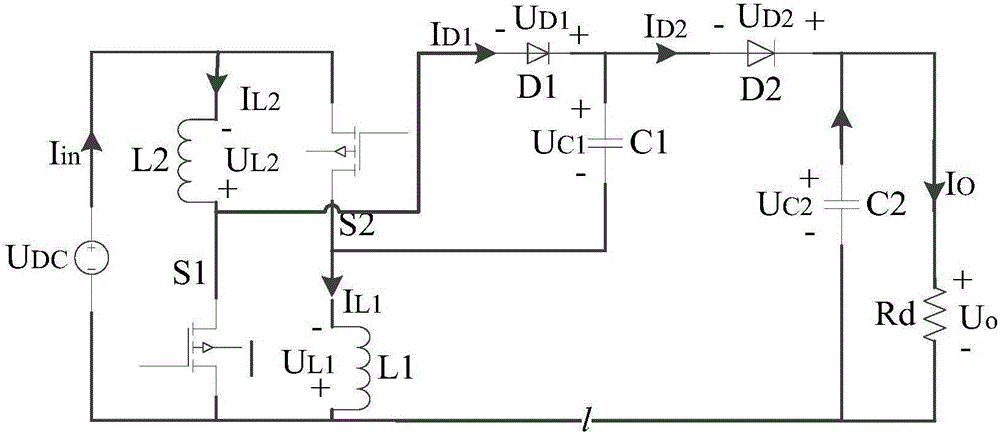
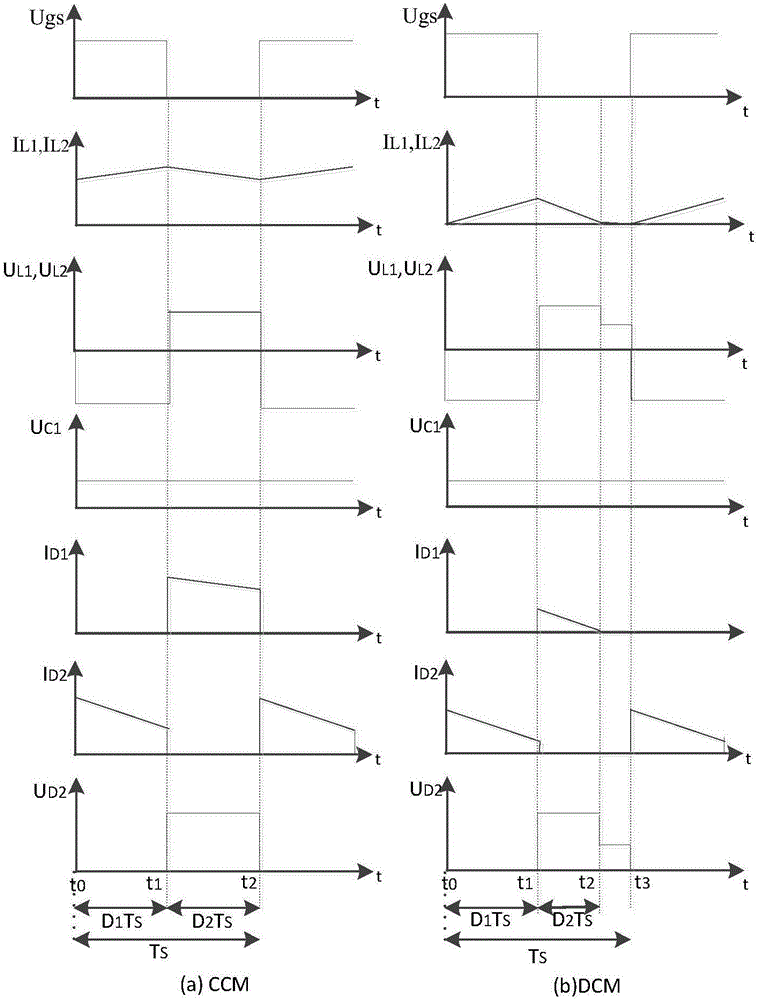
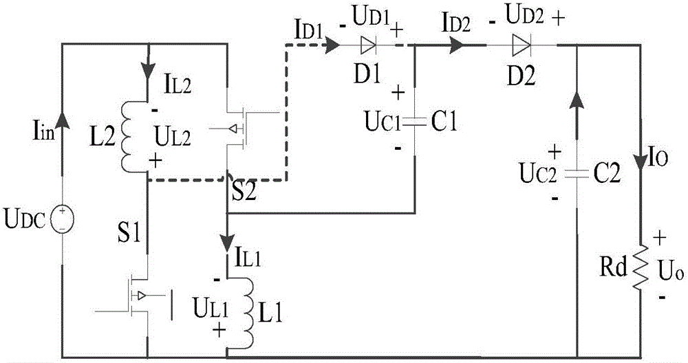
[0033] like figure 1 , which shows the connection of the present non-isolated high-gain DC-DC boost converter topology. The upper end of the switch tube S2 is connected to the upper end of the inductor L2, directly connected to the positive pole of the DC input power supply; the upper end of the inductor L1 is connected to the lower end of the switch tube S2; the upper end of the switch tube S1 is connected to the lower end of the inductor L2; the lower end of the inductor L1 is connected to the lower end of the switch tube S1 The lower end is connected directly to the negative pole of the DC input power supply; the positive pole of the diode D1 is connected to the lower end of the inductor L2, and the negative pole is connected to the positive pole of the capacitor C1 and the positive pole of the diode D2; the negative pole of the capacitor C1 is connected to the lower end of the switch tube S2, and the positive pole and The anode of the diode D2 is connected; the anode of th...
Embodiment 2
[0044] like figure 1 , which shows the connection of the present non-isolated high-gain DC-DC boost converter topology. The upper end of the switch tube S2 is connected to the upper end of the inductor L2, directly connected to the positive pole of the DC input power supply; the upper end of the inductor L1 is connected to the lower end of the switch tube S2; the upper end of the switch tube S1 is connected to the lower end of the inductor L2; the lower end of the inductor L1 is connected to the lower end of the switch tube S1 The lower end is connected directly to the negative pole of the DC input power supply; the positive pole of the diode D1 is connected to the lower end of the inductor L2, and the negative pole is connected to the positive pole of the capacitor C1 and the positive pole of the diode D2; the negative pole of the capacitor C1 is connected to the lower end of the switch tube S2, and the positive pole and The anode of the diode D2 is connected; the anode of th...
PUM
 Abstract
Description
Claims
Application Information
 - Generate Ideas
- Intellectual Property
- Life Sciences
- Materials
- Tech Scout
- Unparalleled Data Quality
- Higher Quality Content
- 60% Fewer Hallucinations
Browse by: Latest US Patents, China's latest patents, Technical Efficacy Thesaurus, Application Domain, Technology Topic, Popular Technical Reports.
© 2025 PatSnap. All rights reserved.Legal|Privacy policy|Modern Slavery Act Transparency Statement|Sitemap|About US| Contact US: help@patsnap.com