PERC (Passivated Emitter and Rear Contact) solar cell
A technology for solar cells and back electrodes, applied in the field of solar cells, can solve the problems of only front power gain at the component end, unable to achieve power gain, large consumption of printing aluminum paste, etc., to improve cell conversion efficiency, reduce contact recombination, The effect of reducing battery costs
- Summary
- Abstract
- Description
- Claims
- Application Information
AI Technical Summary
Problems solved by technology
Method used
Image
Examples
Embodiment 1
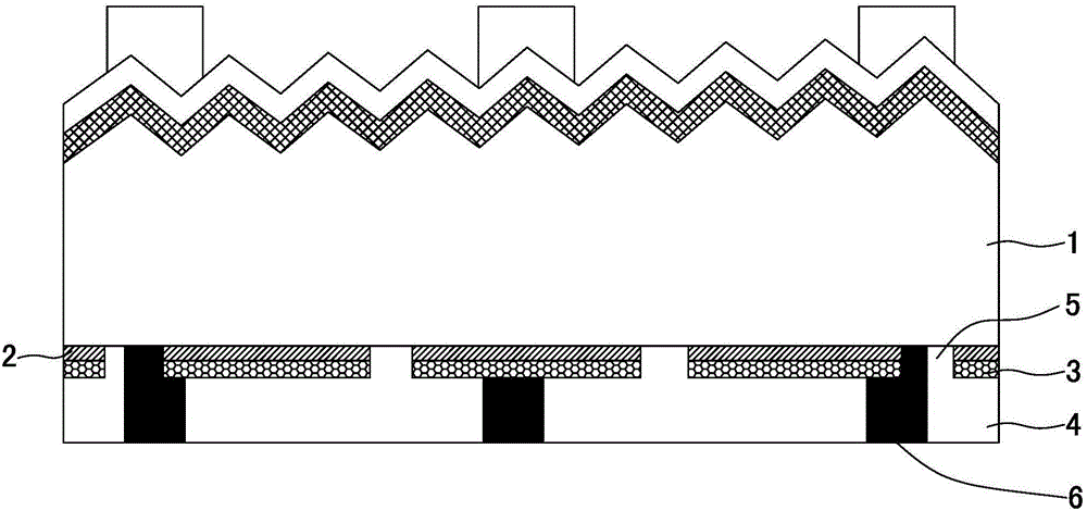
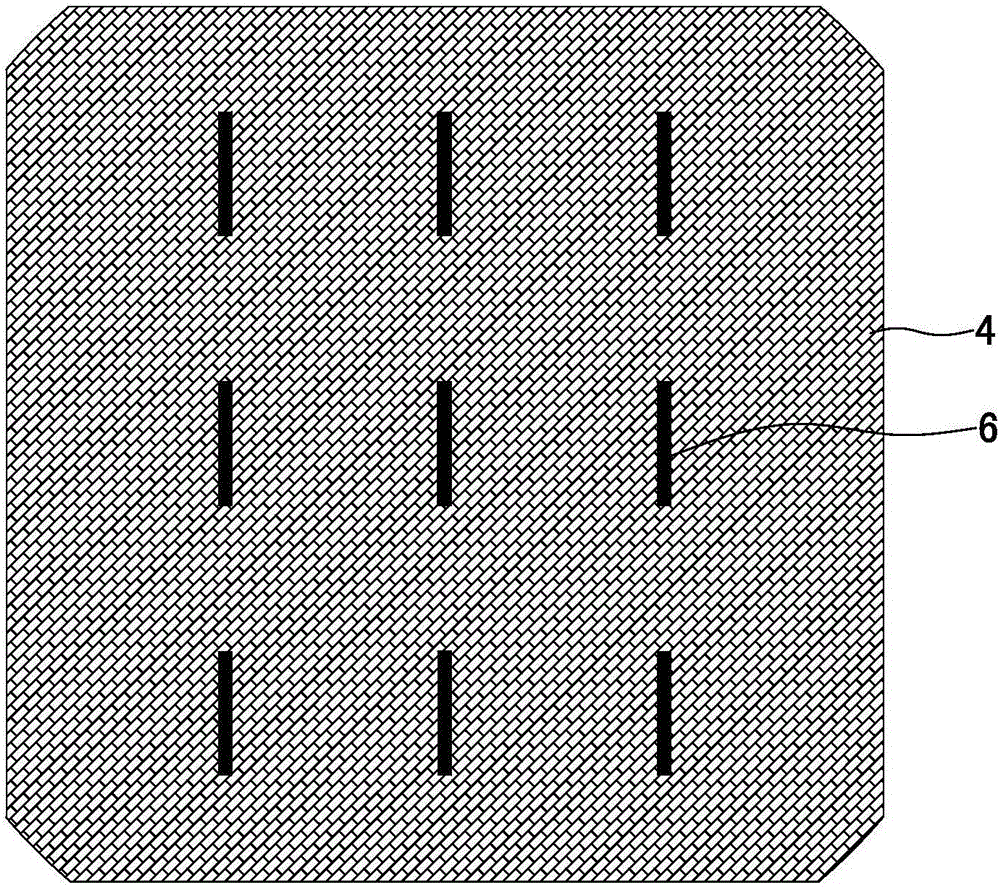
[0038] see Figure 3~4 As shown, a PERC solar cell includes a silicon wafer layer 1 with a PN junction, and a passivation layer (composed of an aluminum oxide layer 2 and a silicon nitride film layer 3) and an aluminum metal layer sequentially arranged on the back of the silicon wafer layer 4; the passivation layer and the silicon nitride film layer are provided with an opening area 5; the back side of the solar cell is provided with a back electrode 6;
[0039] The aluminum metal layer partially covers the back side of the silicon wafer, and the aluminum metal layer covers all of the passivation layer and the opening area on the silicon nitride film layer;
[0040] In terms of the plane where the silicon wafer is located, the position of the back electrode does not coincide with the position of the opening area.
[0041] The area covered by the aluminum metal layer accounts for 80% of the backside area of the silicon wafer. The aluminum metal layer is distributed in strip...
Embodiment 2
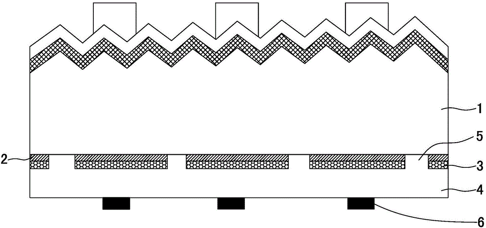
[0045] see Figure 5~6 Shown, a kind of PERC solar cell comprises the silicon slice layer with PN junction, and the passivation layer, silicon nitride thin film layer and aluminum metal layer 4 that are arranged on the backside of silicon slice layer successively; The passivation layer and nitride An opening area is provided on the silicon film layer; a back electrode 6 is provided on the back of the solar cell;
[0046] The aluminum metal layer partially covers the back side of the silicon wafer, and the aluminum metal layer covers all of the passivation layer and the opening area on the silicon nitride film layer;
[0047] The back electrode 6 is in direct contact with the non-opening area of the passivation layer, see Figure 6 shown.
[0048] In terms of the plane where the silicon wafer is located, the position of the back electrode does not coincide with the position of the opening area.
[0049]The area covered by the aluminum metal layer accounts for 60% of the ba...
PUM
 Abstract
Description
Claims
Application Information


