
Electron buffering material and organic electroluminescent device comprising the same

一种电子缓冲、致发光的技术,应用在有机化学、发光材料、电路等方向,能够解决材料群组小、限制、电子缓冲材料受限等问题,达到极佳发光功效、极佳使用寿命特征的效果

Active Publication Date: 2016-11-02
ROHM & HAAS ELECTRONICS MATERIALS KOREA LTD
View PDF22 Cites 17 Cited by
  • Summary
  • Abstract
  • Description
  • Claims
  • Application Information

AI Technical Summary

Problems solved by technology

However, electron-buffering materials are limited to Alq3 derivatives, the group of materials is small, and thus the analysis of effective luminescence efficacy and lifetime improvement is limited

Method used


Image

  • Electron buffering material and organic electroluminescent device comprising the same
  • Electron buffering material and organic electroluminescent device comprising the same
  • Electron buffering material and organic electroluminescent device comprising the same

Examples


example 1

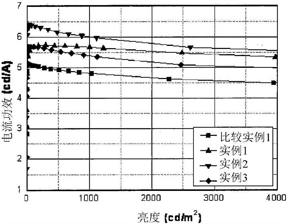
[0130] The measurement results of driving voltage, luminous efficacy, CIE color coordinates, and service life of Examples 1 to 3 and Comparative Example 1, and LUMO and HOMO values ​​of the electron buffer layer are shown in Table 1.

[0131] [Table 1]

[0132]

[0133]

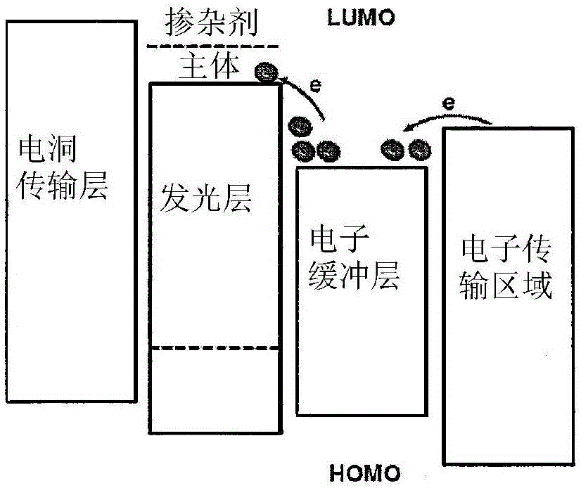
[0134] In Examples 1 to 3, the median value of the LUMO energy level of the electron buffer layer was 1.9 eV or higher, so that the electron injection barrier at the interface between the light emitting layer and the electron buffer layer was minimized to exhibit fast electron injection characteristics, Simultaneously exhibits similar voltage characteristics compared to Comparative Example 1. Specifically, the LUMO levels of Examples 1 and 2 were maintained at 1.8 eV and suitable electron injection characteristics were obtained in order to exhibit high efficacy. On the contrary, the service life of Examples 1 to 3 was similar to that of Comparative Example 1.

[0135] Examples 4 to 7: Organic electr...

example 4

[0139] The measurement results of driving voltage, luminous efficacy, CIE color coordinates, and service life of Examples 4 to 7 and Comparative Example 1, and LUMO and HOMO values ​​of the electron buffer layer are shown in Table 2.

[0140] [Table 2]

[0141]

[0142] In Examples 4 to 7, the LUMO level of the electron buffer layer is between the middle value of 1.9's eV and the high value of 2.0 eV, so that the electron injection barrier of the interface between the light emitting layer and the electron buffer layer has a large influence, and Slow electron injection characteristics were thus exhibited compared to Comparative Example 1. However, higher voltage characteristics were exhibited compared to Comparative Example 1. Therefore, injected electrons were relatively insufficient compared to holes, and the possibility of forming excitons decreased, thereby exhibiting lower efficacy compared with Comparative Example 1. However, a longer service life was exhibited compa...

example 8

[0147] The measurement results of driving voltage, luminous efficacy, CIE color coordinates, and service life of Examples 8 to 12 and Comparative Example 1, and the LUMO and HOMO values ​​of the electron buffer layer are shown in Table 3.

[0148] [table 3]

[0149]

[0150] In Examples 8 to 12, the LUMO level of the electron buffer layer was formed at a median value of 1.9 eV, and an electron injection barrier was applied at a certain level so that suitable electron injection characteristics were exhibited, which satisfied the efficacy and service life. Therefore, higher efficacy and longer service life were exhibited compared to Comparative Example 1. Specifically, excellent lifetime characteristics, ie, 1.5% or more higher than that of Comparative Example 1 were exhibited, while exhibiting high efficacy.

[0151] The use of electron buffer layers comprising triazine derivatives is advantageous for proper efficacy and lifetime.

[0152] Examples 13 to 15: Organic elec...


PUM

PropertyMeasurementUnit
wavelengthaaaaaaaaaa

Abstract

The present invention relates to an electron buffering material and an organic electroluminescent device comprising the same in an electron buffer layer. It is possible to provide an organic electroluminescent device having excellent luminous efficiency and lifespan characteristics by using the electron buffering material according to the present invention.

Description

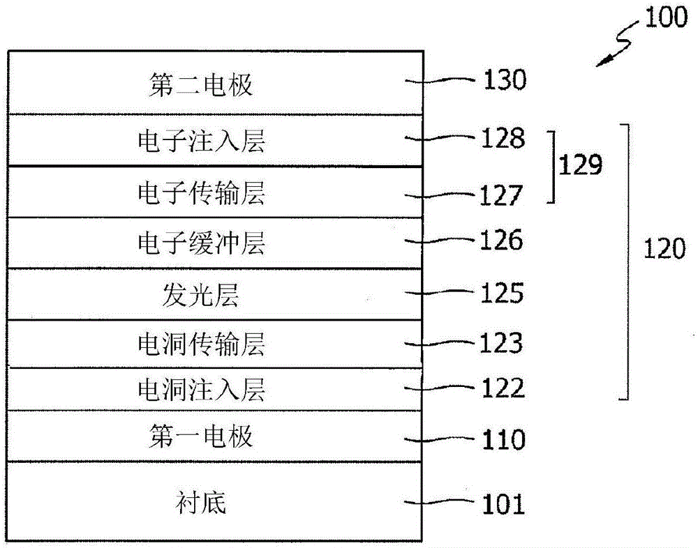
technical field [0001] The present invention relates to electron buffer materials and organic electroluminescent devices comprising them. Background technique [0002] After Tang et al. of Eastman Kodak first developed a TPD / Alq3 double-layer small molecule green organic electroluminescent device (OLED) composed of an emissive layer and an electron transport layer in 1987, research on organic electroluminescent devices has been carried out rapidly and Now commoditized. Currently, phosphorescent materials, which have excellent luminous efficacy, are mainly used in panels of organic electroluminescent devices. Commercialization of organic electroluminescent devices using phosphorescent materials has been successful in the case of red- and green-emitting organic electroluminescent devices, but in the case of blue phosphorescent materials, excessive formation of excitons due to lack The resulting decrease in the decay rate at high current leads to characteristic deterioration,...

Claims


Application Information

Patent Timeline
Patent Type & Authority Applications(China)
IPC IPC(8): C07D403/14C07D409/14C07D403/10C07D405/14C07D403/04C07D495/02C07D487/02C07D491/02C09K11/06H01L27/32H01L51/54
CPCC07D403/12C07D405/14C07D403/04C07D403/14C07D405/04C07D409/14C07D471/04C07D487/04C07D495/04C07D403/10C09K11/025C09K11/06H10K85/654H10K85/6576H10K85/6574H10K85/6572H10K85/657H10K50/157H10K50/18H10K85/30H10K50/12H10K85/615H10K85/626H10K85/633H10K30/865C09K2211/1007C09K2211/1011C09K2211/1014
Inventor S-H·曹J-H·全H-Y·娜J-S·俊J-H·沈K-H·崔C-S·金Y-J·曹
Owner ROHM & HAAS ELECTRONICS MATERIALS KOREA LTD
Learn More