

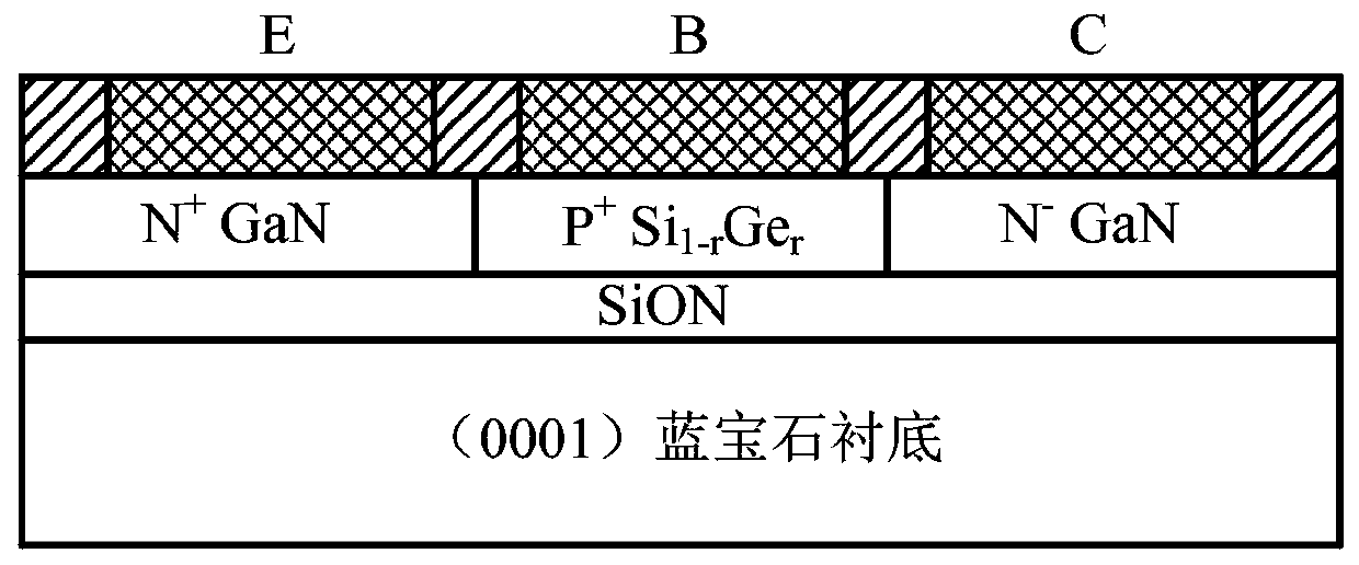
NPN type transverse GaN/SiGe HBT device structure and manufacturing method thereof
A device structure and horizontal technology, applied in semiconductor/solid-state device manufacturing, semiconductor devices, electrical components, etc., can solve unsatisfactory problems, achieve the effect of increasing frequency, reducing transit time, and improving mobility
- Summary
- Abstract
- Description
- Claims
- Application Information
AI Technical Summary
Problems solved by technology
Method used
Image


Examples
Embodiment Construction
[0034] In order to make the technical means, creative features, goals and effects achieved by the present invention easy to understand, the present invention will be further described below in conjunction with specific illustrations.
[0035] In describing the present invention, it is to be understood that the terms "longitudinal", "radial", "length", "width", "thickness", "upper", "lower", "front", "rear", The orientation or positional relationship indicated by "left", "right", "vertical", "horizontal", "top", "bottom", "inner", "outer", etc. is based on the orientation or positional relationship shown in the drawings , is only for the convenience of describing the present invention and simplifying the description, but does not indicate or imply that the referred device or element must have a specific orientation, be constructed and operated in a specific orientation, and thus should not be construed as limiting the present invention. In the description of the present inventi...
PUM
| Property | Measurement | Unit |
|---|---|---|
| thickness | aaaaa | aaaaa |
| thickness | aaaaa | aaaaa |
| thickness | aaaaa | aaaaa |
Abstract
Description
Claims
Application Information