vtft with polymer core
A technology of polymer materials and electrodes, applied in semiconductor devices, electrical components, transistors, etc.
- Summary
- Abstract
- Description
- Claims
- Application Information
AI Technical Summary
Problems solved by technology
Method used
Image

Examples
Embodiment
[0168] Description of coating device
[0169] The method for depositing the inorganic thin film layer of following embodiment all adopts as reference Figure 66 The flow setup (flowsetup). The flow path setup is supplied with a nitrogen stream 81 which has been purified to remove oxygen and water impurities to below 1 ppm. The gas is diverted through a manifold to several flow meters that control the flow of purge gas and gas diverted through the bubbler to select reactive precursors. In addition to the nitrogen supply, an air stream 90 is delivered to the plant. The air is preconditioned to remove moisture.
[0170] The following streams are delivered to the ALD coating apparatus: a metal (zinc) precursor stream 92 containing a metal precursor diluted in nitrogen; an oxidant-containing stream 93 containing a non-metallic precursor or an oxidant diluted in nitrogen; and only A nitrogen purge stream 95 consisting of an inert gas. The composition and flow of these streams...
Embodiment I1
[0200] Inventive Example I1: Quad Pixel with Printed VTFTF
[0201] In order to manufacture the inventive example I1, a glass substrate was provided and an O 2Plasma (100W 0.3 Torr for 1 minute) cleaning. Next, a solution of 40 wt% SU-8 2010 in cyclopentanone was spun at 500 rpm for 10 seconds and ramped up to 2000 rpm for a final 30 seconds. The coating was made using a pre-exposure hot plate bake of two minutes at 95°C, a blanket exposure of 90 seconds, a post-exposure hot plate bake of two minutes at 95°C and a final hard bake at 225°C. A baked recipe was used to cure, resulting in a cured SU-8 film at 7500 Å.
[0202] Next, the surface of SU-8 was coated with O 2 Plasma treatment for 30 seconds to activate the surface of SU-8. An inorganic cap was formed over the SU-8 layer using a combination of SAD and ALD. Selective area deposition was performed using a patterned layer of deposition inhibiting material using a Fuji Dimatix 2500 piezo inkjet printer as described w...
Embodiment I2
[0210] Inventive Example I2: Triple Pixel with Printed VTFT Layer
[0211] Inventive Example I2 was formed using the same process as Inventive Example I1 and on the same substrate. The only difference between Inventive Embodiment I2 and I1 is that Inventive Embodiment I2 has a 3-pixel wide pattern, which is used to define the width of the transistor when forming the source and drain electrodes.
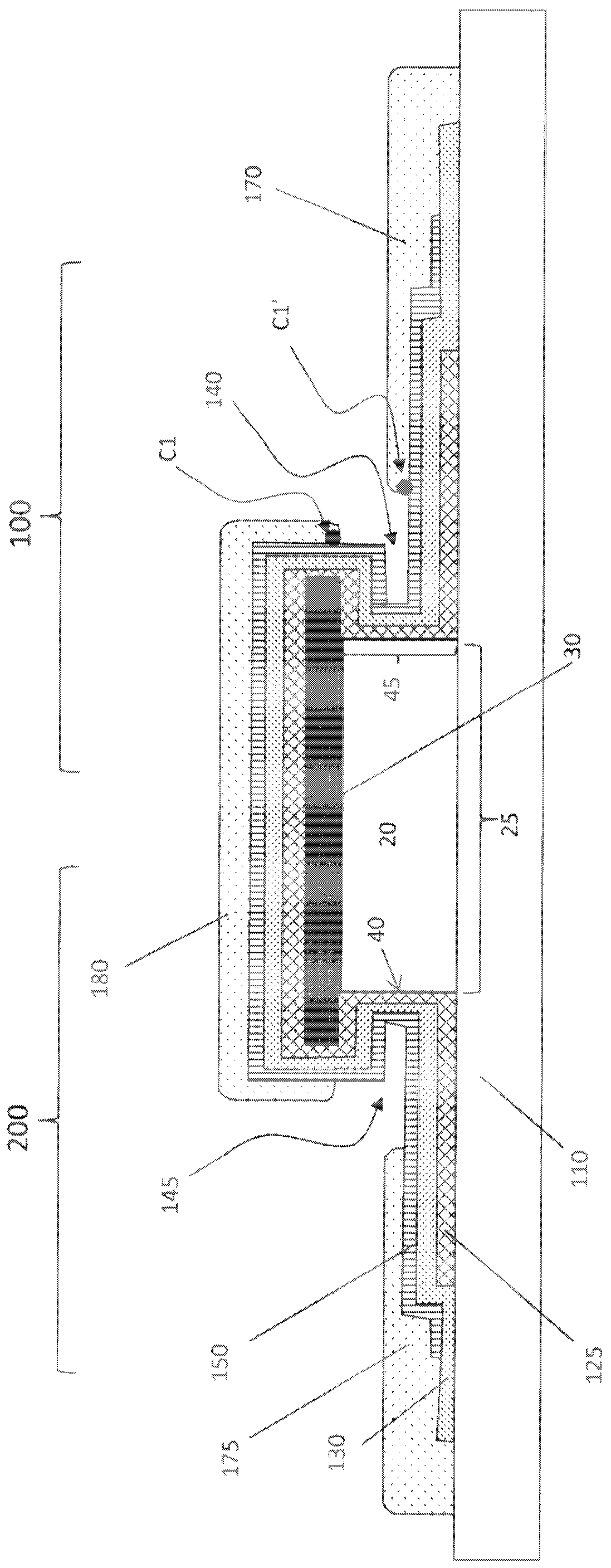
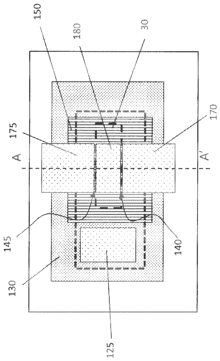
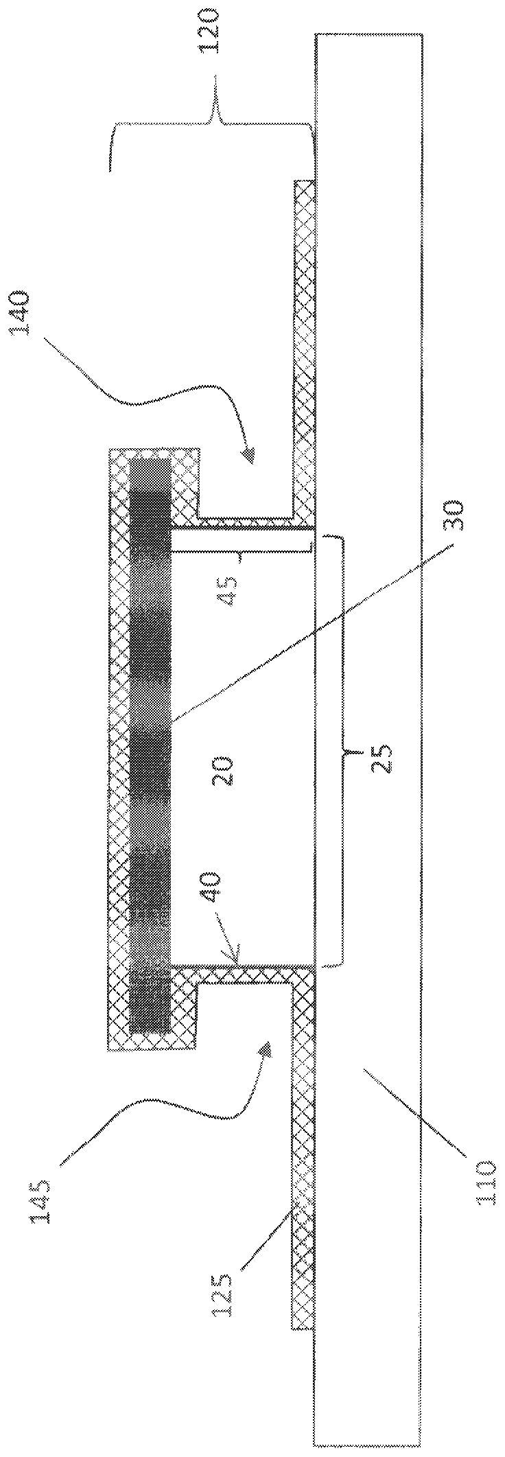
[0212] The VTFT of Example I2 of the present invention is shown in Figs. 68a to 68c. Figure 68a is an optical micrograph of a complete VTFT. For easy understanding, the first, second and third electrodes (180, 170 and 175) are as Figure 1b marked in. The post and cover structures are identified by the outline of the cover 30 . Figure 68a is an optical micrograph illustrating features of the present invention, wherein a channel is defined by a first electrode and a second electrode comprising a width dimension and a length dimension, wherein the length dimension varies along the...
PUM
 Abstract
Description
Claims
Application Information
 - R&D
- Intellectual Property
- Life Sciences
- Materials
- Tech Scout
- Unparalleled Data Quality
- Higher Quality Content
- 60% Fewer Hallucinations
Browse by: Latest US Patents, China's latest patents, Technical Efficacy Thesaurus, Application Domain, Technology Topic, Popular Technical Reports.
© 2025 PatSnap. All rights reserved.Legal|Privacy policy|Modern Slavery Act Transparency Statement|Sitemap|About US| Contact US: help@patsnap.com