Three-dimensional power VDMOS device and integration method thereof

A three-dimensional power and integration method technology, applied in the fields of semiconductor devices, electric solid-state devices, semiconductor/solid-state device manufacturing, etc., can solve the problems affecting the integration of power systems, signal delay time, and the power consumption ratio of interconnect lines, and achieve shortening The effect of signal delay time, shortening the length of global interconnection lines, and reducing the proportion of power consumption

Active Publication Date: 2016-11-09
GUIZHOU UNIV
View PDF8 Cites 4 Cited by
  • Summary
  • Abstract
  • Description
  • Claims
  • Application Information

AI Technical Summary

Problems solved by technology

[0004] The technical problem to be solved by the present invention is to provide a three-dimensional power VDMOS device and its integration method, so as to solve the problem that the device area of ​​the prior art VDMOS device adopts the planar integration process increases with the increase of the current capacity, which seriously affects the power system The level of integration, while the signal delay time and the proportion of interconnection power consumption will also become more and more technical issues such as

Method used


Image

  • Three-dimensional power VDMOS device and integration method thereof

Examples


Embodiment Construction

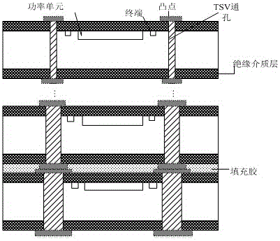
[0034] A three-dimensional power VDMOS device, which includes a power unit and a chip layer, the chip layer has more than two, each chip layer is evenly distributed with more than two power units, and each power unit is provided with an independent terminal on the periphery, The periphery of each power unit is provided with TSV through holes for interlayer conductive interconnection, and each chip layer is stacked together to form a three-dimensional power VDMOS device.

[0035] TSV through holes for heat dissipation are arranged on the periphery of the power unit. Embed heat-dissipating TSV vias around the periphery of each power unit, the number of which is related to the power loss of each power unit, the aspect ratio of the TSV vias, and the thickness of the insulating layer in the TSV vias;

[0036] Since the drain current of the VDMOS power unit of each chip layer passes through the TSV through hole of the interlayer conductive interconnection and finally gathers on the ...


PUM


Abstract

The invention discloses a three-dimensional power VDMOS device and an integration method thereof. The three-dimensional power VDMOS device comprises power units and two or more chip layers, wherein two or more power units are uniformly distributed on each chip layer, an independent terminal is arranged on the periphery of each power unit, interlayer conductive interconnecting TSV through holes are arranged in the periphery of each power unit, and chip layers stack together to form the three-dimensional power VDMOS device. The technical problems that since a VDMOS device employs a plane integration technology, the area of the device increases with the increasing of the current capacity, the integration level of a power system is severely affected, and signal delay time and interconnection line power consumption proportion are greater can be solved.

Description

technical field [0001] The invention belongs to VDMOS device integration technology, in particular to a three-dimensional power VDMOS device and an integration method thereof. Background technique [0002] As one of the main components in power electronic equipment, power VDMOS devices are mainly used to realize the conversion of electric energy. It is a new type of power device developed rapidly in the 1980s. Compared with bipolar power devices, it has many excellent properties: high input impedance, low drive current, high speed and high frequency, negative current temperature coefficient, no secondary breakdown, etc. Moreover, the drain of VDMOS is drawn from the back, and its integration level is higher than that of power LDMOS. , the interface circuit between the control circuit and the power load, etc. [0003] At present, the manufacturing process of power VDMOS devices still uses the traditional planar integration process, and the active layer of the device only ex...

Claims


Application Information

Patent Timeline
Patent Type & Authority Applications(China)
IPC IPC(8): H01L27/088H01L29/78H01L23/367H01L23/538H01L21/336H01L21/8234
CPCH01L23/5384H01L27/088H01L29/66712H01L29/7802H01L21/823475H01L23/3677H01L2224/16145
Inventor 林洁馨傅兴华马奎杨发顺
Owner GUIZHOU UNIV
Why Eureka
Try Eureka