Multi-wavelength array laser and manufacture method and use method thereof
A manufacturing method and laser technology, applied in the field of lasers, can solve the problems of limiting the use of electron beam lithography, expensive processing costs, and long processing time, and achieve the effects of ensuring laser wavelength coverage, strong wavelength correction capabilities, and small crosstalk
- Summary
- Abstract
- Description
- Claims
- Application Information
AI Technical Summary
Problems solved by technology
Method used
Image

Examples
Embodiment 1
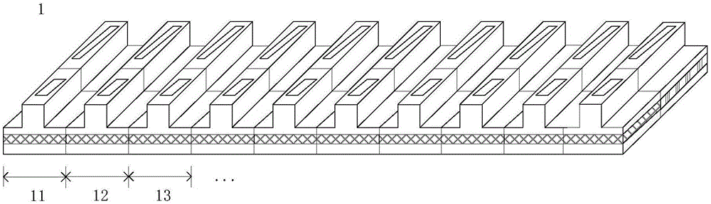
[0067] Embodiment 1 of the present invention provides a multi-wavelength array laser, such as image 3 As shown, including at least two distributed Bragg reflection lasers (such as image 3 As shown, including distributed Bragg reflection laser 11, distributed Bragg reflection laser 12, distributed Bragg reflection laser 13...), reference Figure 4 , each distributed Bragg reflection laser includes an active region structure 111 and a grating region structure 112, such as Figure 3-Figure 5 Shown:
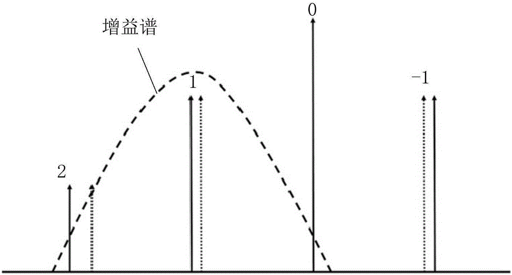
[0068] The grating region structure 112 of each DBR laser includes one or more grating regions, and each grating region is separated by a specified length. Wherein, gratings with the same grating period Λ are used to form the grating area in each distributed Bragg reflection laser.
[0069] The grating area is separated by a specified length as the sampling length L in the figure S After subtracting the length Lg of the grating area in the figure, it is obtained by Figure 5 A...
Embodiment 2
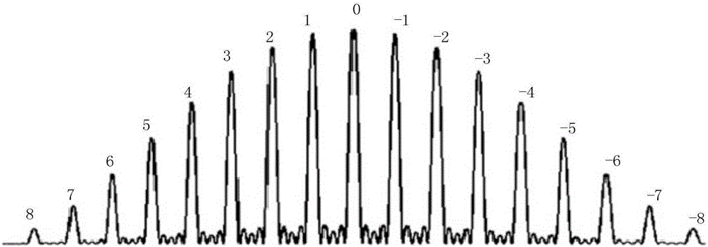
[0088] Embodiment 1 of the present invention introduces a multi-wavelength array laser, and analyzes the feasibility of a multi-wavelength array laser proposed by the present invention in principle by combining the technical problems described in the background technology, and The problems that may be encountered in the implementation process and the aspects that can be optimized are partially described. Embodiment 2 of the present invention is based on the above-mentioned embodiment 1, and the last mentioned situation may not be able to achieve the expected accuracy. After research, it is found that the overall structure of the grating region can be changed by supplying power to the electrodes in the grating region structure. Effective refractive index, so that each reflection peak of the grating comb reflection spectrum can be adjusted within a controllable range to complete translation within a small range. Therefore, another realizable solution is provided. Compared with t...
Embodiment 3
[0094] On the basis that Embodiment 1 provides a multi-wavelength array laser, the present invention also provides Embodiment 3: a manufacturing method of a multi-wavelength array laser, which can be used to manufacture such as Embodiment 1 or Embodiment 2. The multi-wavelength array laser, such as Figure 10 As shown, the manufacturing method includes the following steps:
[0095] In step 201, the active area structure part and / or the phase area structure part of each distributed Bragg reflector laser used to make the multi-wavelength array laser is masked on the wafer, and the grating area is formed by using the holographic exposure method The structure part etches grating areas with the same grating period; wherein, the interval of each grating area in each distributed Bragg reflection laser is set according to the wavelength to be lased;
[0096] In step 202, the active region structure is grown in the active region structure, the grating region structure is grown in the ...
PUM
 Abstract
Description
Claims
Application Information
 - R&D
- Intellectual Property
- Life Sciences
- Materials
- Tech Scout
- Unparalleled Data Quality
- Higher Quality Content
- 60% Fewer Hallucinations
Browse by: Latest US Patents, China's latest patents, Technical Efficacy Thesaurus, Application Domain, Technology Topic, Popular Technical Reports.
© 2025 PatSnap. All rights reserved.Legal|Privacy policy|Modern Slavery Act Transparency Statement|Sitemap|About US| Contact US: help@patsnap.com