

Semiconductor device and manufacturing method thereof
A manufacturing method and semiconductor technology, applied in the direction of semiconductor devices, semiconductor/solid-state device manufacturing, semiconductor/solid-state device components, etc., can solve the problems of semiconductor device electrical characteristic degradation and failure
- Summary
- Abstract
- Description
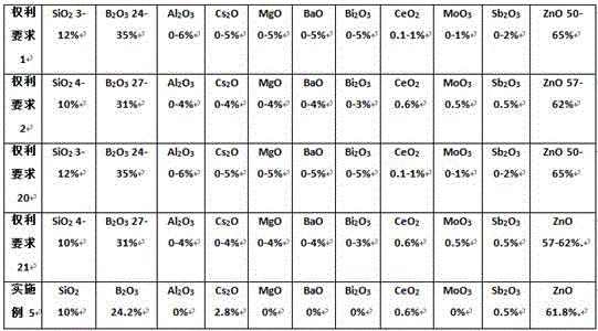
- Claims
- Application Information
AI Technical Summary
Problems solved by technology
Method used
Image

Examples
Embodiment Construction
[0016] Embodiments of the present invention will be described in detail below with reference to the accompanying drawings.
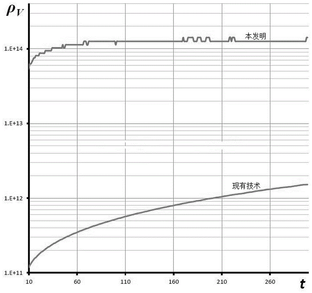
[0017] A semiconductor device using a glass passivation layer based on aluminosilicate, such as lead oxide (PbO) or (ZnO) zinc oxide aluminosilicate. In order to increase the reliability of the semiconductor device under reverse bias and high temperature thermal stress, the aluminosilicate glass passivation layer contains cesium at a concentration of 20ppm (mol, mole percent) to 200ppm (mol, mole percent).
[0018] The results of XPS (X-ray photoelectron spectroscopy, X-ray photoelectron spectroscopy) technology measurement show that the concentration of cesium on the surface of the glass passivation layer is consistent with the setting of the present invention, specifically 5*10 18 cm -3 . We compare the resistivity of the glass passivation layer (measured using ASTM D-257) to 2*10 11 Ω·cm - 3*10 11 The range of Ω·cm has been increased to 1.5*10 ...
PUM
 Abstract
Description
Claims
Application Information