Semiconductor device and forming method thereof

A semiconductor and device technology, applied in the field of semiconductor manufacturing, can solve the problems of short channel effect, large leakage current, etc., achieve the effects of reducing leakage current, increasing source-drain breakdown voltage, and improving short channel effect

Inactive Publication Date: 2016-11-23
SEMICON MFG INT (SHANGHAI) CORP
View PDF5 Cites 5 Cited by
  • Summary
  • Abstract
  • Description
  • Claims
  • Application Information

AI Technical Summary

Problems solved by technology

[0005] However, in practical applications, it is found that the semiconductor devices formed by the

Method used


Image

  • Semiconductor device and forming method thereof
  • Semiconductor device and forming method thereof
  • Semiconductor device and forming method thereof

Examples


Embodiment Construction

[0034] It can be seen from the background art that the semiconductor devices formed in the prior art have significant short channel effect, low source-drain breakdown voltage, and large leakage current.

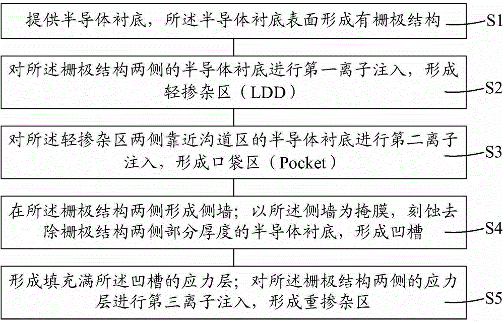
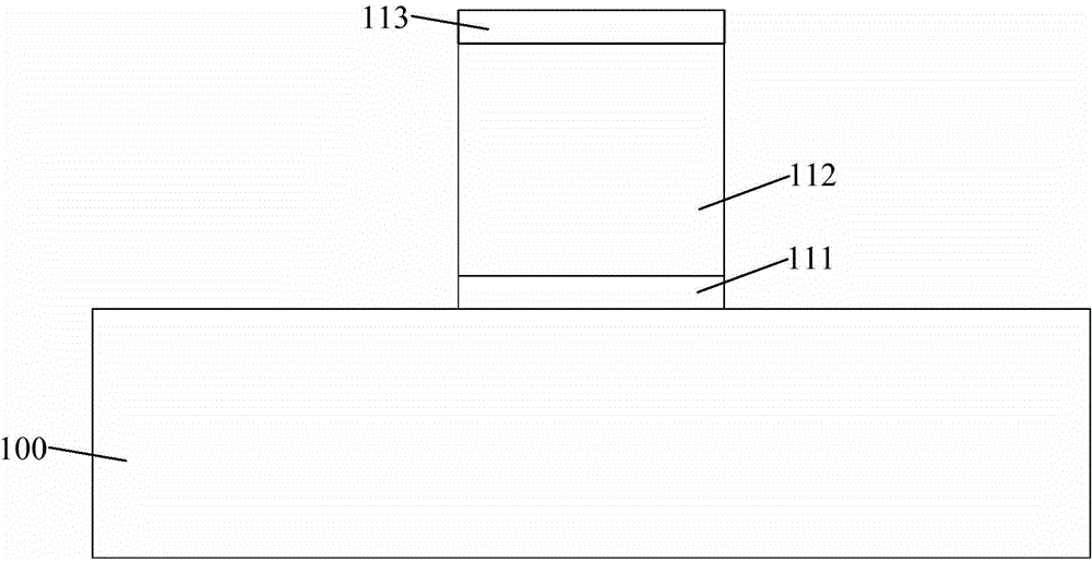
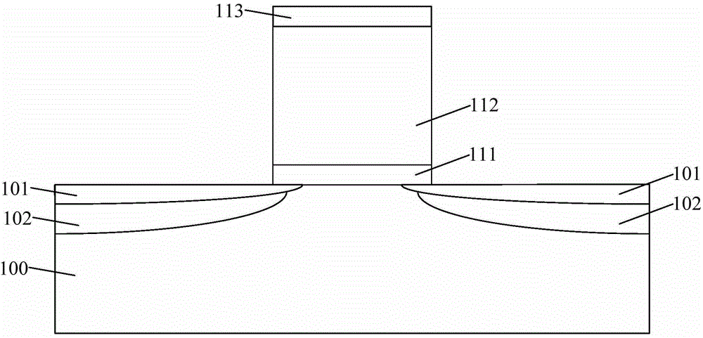
[0035] After research, it is found that the formation process of semiconductor devices includes the following steps, please refer to figure 1 : Step S1, providing a semiconductor substrate, the surface of the semiconductor substrate is formed with a gate structure; Step S2, carrying out the first ion implantation to the semiconductor substrate on both sides of the gate structure, forming a lightly doped region (LDD) ; Step S3, performing second ion implantation on the semiconductor substrate on both sides of the lightly doped region close to the channel region to form a pocket region (Pocket); Step S4, forming sidewalls on both sides of the gate structure; The sidewall is a mask, and the semiconductor substrate on both sides of the gate structure is etched and removed to form...


PUM

PropertyMeasurementUnit
Thicknessaaaaaaaaaa
Thick bottomaaaaaaaaaa

Abstract

The invention provides a semiconductor device and a forming method thereof. The forming method of the semiconductor device comprises the steps of providing a substrate, wherein a gate structure is formed on the surface of the substrate; etching a certain thickness part of the substrate on the two sides of the gate structure so as to form a groove in the substrate; forming a diffusion barrier layer on the surface of the sidewall of the groove that is close to the gate structure; forming a stress layer on the surface of the diffusion barrier layer to fill the groove with the stress layer; conducting the doping treatment on the stress layer and forming a heavily doped region in the stress layer. According to the technical scheme of the invention, doped ions in the heavily doped region are prevented from being diffused into the substrate under the gate structure, so that the short-channel effect is improved. Meanwhile, the source/drain breakdown voltage is increased and the leakage current of the semiconductor device is reduced.

Description

technical field [0001] The invention relates to the technology in the field of semiconductor manufacturing, in particular to a semiconductor device and a forming method thereof. Background technique [0002] With the continuous development of semiconductor technology, carrier mobility enhancement technology has been widely studied and applied. Improving the carrier mobility in the channel region can increase the driving current of semiconductor devices and improve the performance of devices. [0003] In the existing manufacturing process of semiconductor devices, since stress can change the energy gap and carrier mobility of silicon materials, it has become more and more common means to improve the performance of semiconductor devices through stress. Specifically, by properly controlling the stress, the mobility of carriers (electrons in NMOS devices, holes in PMOS devices) can be increased, thereby increasing the driving current, thereby greatly improving the performance of...

Claims


Application Information

Patent Timeline
IPC IPC(8): H01L21/336H01L29/78H01L29/06
Inventor 赵猛
Owner SEMICON MFG INT (SHANGHAI) CORP
Why Eureka
Try Eureka