Formation method of semiconductor structure

A semiconductor and gate structure technology, applied in the field of semiconductor structure formation, can solve problems affecting the performance of semiconductor devices, poor stress layer morphology, etc., and achieve the effects of avoiding defects, improving performance and yield, and avoiding leakage current

Active Publication Date: 2019-04-26
SEMICON MFG INT (SHANGHAI) CORP
View PDF6 Cites 0 Cited by
  • Summary
  • Abstract
  • Description
  • Claims
  • Application Information

AI Technical Summary

Problems solved by technology

[0004] However, the stress layer formed by the prior art has poor morphology, which easily affects the performance of semiconductor devices

Method used


Image

  • Formation method of semiconductor structure
  • Formation method of semiconductor structure
  • Formation method of semiconductor structure

Examples


Embodiment Construction

[0034] As mentioned in the background art, the stress layer formed in the prior art has poor morphology, which easily affects the performance of semiconductor devices.

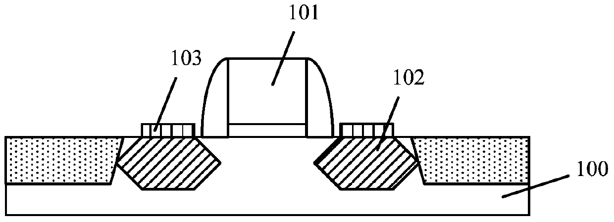
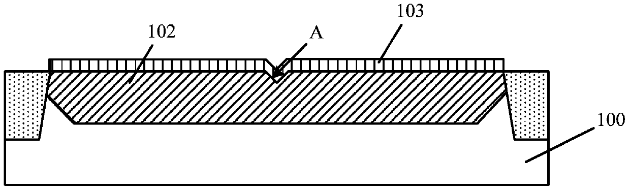
[0035] Please refer to figure 1 , figure 1 It is a schematic cross-sectional structure diagram of a transistor embodiment, including: a substrate 100; a gate structure 101 located on the surface of the substrate 100; a stress layer 102 located on both sides of the gate structure 101; P-type ions or N-type ions form a source region and a drain region; and a covering layer 103 located on the surface of the stress layer 102 .

[0036] Wherein, the cover layer 103 is used to be converted into an electrical contact layer in a subsequent metal silicide process, and the material of the electrical contact layer is a metal silicide material. Since it is necessary to form an electrical interconnection structure, such as a conductive plug, on the surface of the source region and the drain region, the electrical contact...


PUM

PropertyMeasurementUnit
thicknessaaaaaaaaaa
thicknessaaaaaaaaaa
thicknessaaaaaaaaaa

Abstract

The invention provides a semiconductor structure forming method. The method comprises the steps of providing a substrate; forming an opening in the substrate; forming a stress layer in the opening; forming an initial covering layer on the surface of the substrate and the surface of the stress layer, wherein the material of the initial covering layer is composed of an amorphous semiconductor material; converting the part of the initial covering layer, that is positioned on the surface of the stress layer, into a covering layer through the crystallization process, wherein the material of the covering layer is composed of a crystalline semiconductor material; and removing the initial covering layer that is not converted into the covering layer after the crystallization process. The formed semiconductor structure is good in morphology and stable in performance.

Description

technical field [0001] The invention relates to the technical field of semiconductor manufacturing, in particular to a method for forming a semiconductor structure. Background technique [0002] With the rapid development of semiconductor manufacturing technology, semiconductor devices are developing towards higher component density and higher integration. Transistors are currently being widely used as the most basic semiconductor devices, so as the element density and integration of semiconductor devices increase, the gate size of transistors has become shorter than before. However, the shortening of the gate size of the transistor will cause the short-channel effect of the transistor, thereby generating leakage current, and ultimately affecting the electrical performance of the semiconductor device. At present, the prior art mainly improves the performance of semiconductor devices by increasing carrier mobility. When the mobility of carriers is increased, the driving cur...

Claims


Application Information

Patent Timeline
Patent Type & Authority Patents(China)
IPC IPC(8): H01L21/336H01L21/02H01L29/78
CPCH01L21/02365H01L21/02675H01L29/66636H01L29/7848
Inventor 禹国宾
Owner SEMICON MFG INT (SHANGHAI) CORP
Why Eureka
Try Eureka