Formation method of semiconductor structure
A semiconductor and gas technology, applied in semiconductor/solid-state device manufacturing, electrical components, circuits, etc., can solve the problems of metal plug contact performance to be improved, achieve good side wall morphology, improve etching efficiency, and increase contact area big effect
- Summary
- Abstract
- Description
- Claims
- Application Information
AI Technical Summary
Problems solved by technology
Method used
Image
Examples
Embodiment Construction
[0039] As mentioned in the background art, the contact performance between the copper metal wire and the metal plug at the bottom still needs to be improved.
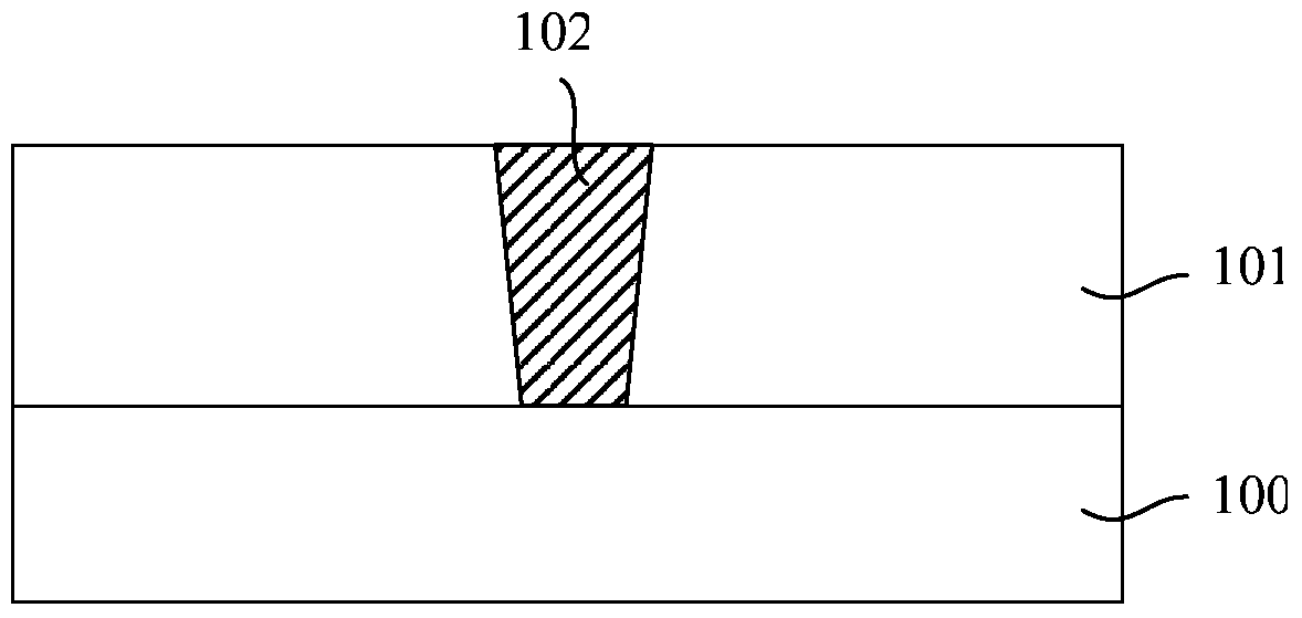
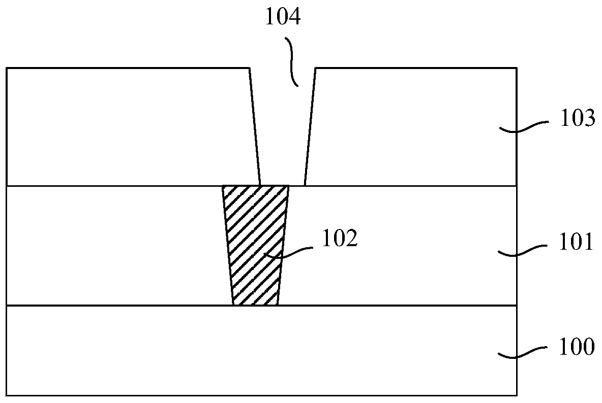
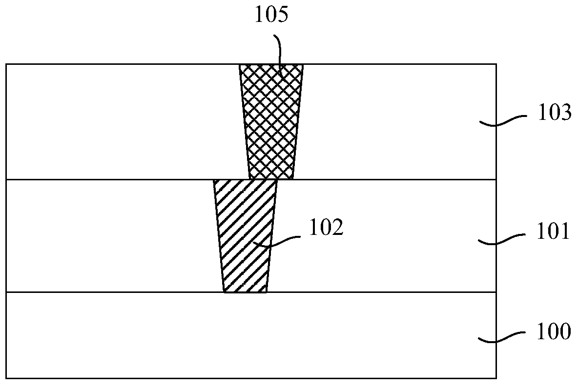
[0040] Research has found that in the prior art, an electroplating process is usually used to form copper metal lines, that is, an opening is formed in the second dielectric layer, and then an electroplating process is used to fill the opening with copper to form a copper metal line. However, as the feature size continues to decrease, when the second dielectric layer is patterned, the position of the opening formed due to the limitation of the photolithography process is likely to shift, and due to the limitation of the etching process, the bottom of the formed opening The width will be smaller than that of the top, and when the copper metal line is formed in the opening, the contact area between the copper metal line and the metal plug at the bottom will be reduced, which affects the electrical performance of the formed...
PUM
| Property | Measurement | Unit |
|---|---|---|
| temperature | aaaaa | aaaaa |
| pressure | aaaaa | aaaaa |
| thickness | aaaaa | aaaaa |
Abstract
Description
Claims
Application Information


