

Method for simultaneously fabricating semiconductor elements in unit cell region and surrounding region
A technology of unit cell area and surrounding area, which is applied in semiconductor devices, semiconductor/solid-state device manufacturing, electrical components, etc., can solve problems such as damage to extremely thin oxide layers, and achieve the effect of reducing the risk of oxide layer damage
- Summary
- Abstract
- Description
- Claims
- Application Information
AI Technical Summary
Problems solved by technology
Method used
Image

Examples
Embodiment Construction
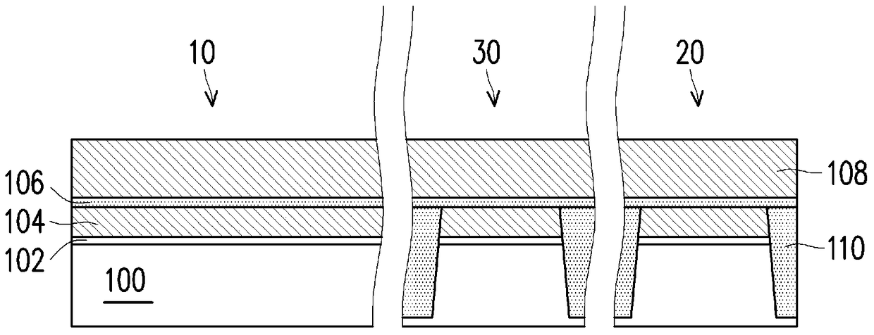
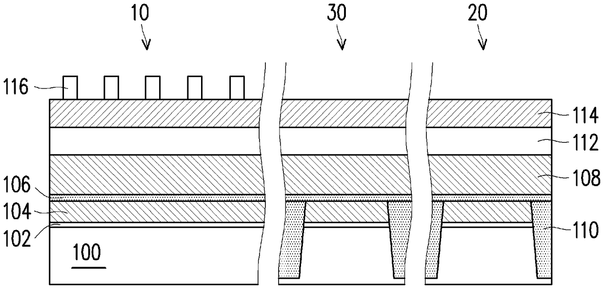
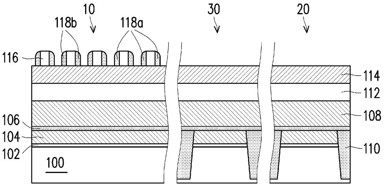
[0050] Figure 1A to Figure 1H It is a schematic cross-sectional view of a manufacturing process of a semiconductor device in which a unit cell region and a surrounding region are simultaneously manufactured according to the first embodiment of the present invention.
[0051] Please refer to Figure 1A , a substrate 100 is provided, and the substrate 100 has a unit cell area 10 and a surrounding area 20 . There is also a capacitor region 30 in the substrate 100 of the present embodiment. Although there is only one unit cell region 10 , surrounding region 20 and capacitor region 30 in the figure, the present invention is not limited thereto. Then, a gate oxide layer 102 , a first conductive structure layer 104 , an inter-gate dielectric layer 106 and a second conductive structure layer 108 are sequentially formed on the substrate 100 . The first conductive structure layer 104 is, for example, a single-layer or double-layer structure made of tungsten, aluminum, copper, polysil...
PUM
 Abstract
Description
Claims
Application Information