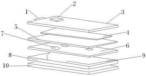
Circuit board structure with cooling function
A technology of circuit boards and functions, which is applied in the direction of printed circuits, printed circuits connected with non-printed electrical components, circuit heating devices, etc., can solve the problems of low cost and inability to apply products, so as to improve the use performance and improve the use performance and the effect of service life
- Summary
- Abstract
- Description
- Claims
- Application Information
AI Technical Summary
Problems solved by technology
Method used
Image
Examples
Embodiment 1
[0024] A circuit board structure with built-in heat dissipation function. A heat dissipation layer is set at the bottom of the circuit board structure to dissipate heat for the entire circuit board structure, effectively improving the performance of the circuit board structure, and adopting layered setting technology for different The circuit components of power consumption are packaged in layers, so as to effectively improve the performance and service life of the entire circuit structure, such as figure 1 As shown, the following structure is particularly arranged: a substrate layer 8, a semiconductor device mounting layer 6, an insulating layer 5, and a chip mounting layer 3 are provided, and a semiconductor device mounting layer 6 is arranged on one side of the substrate layer 8, and the insulating layer 5 is arranged on the opposite surface of the substrate layer 8 on the semiconductor device mounting layer 6, and the chip mounting layer 3 is arranged on the opposite surfac...
Embodiment 2
[0027] This embodiment is further optimized on the basis of the above-mentioned embodiments. Further, in order to better realize the present invention, it can facilitate the connection of various components of the circuit, such as figure 1 As shown, the following arrangement structure is particularly adopted: on the surface of the substrate layer 8 that is in contact with the semiconductor device mounting layer 6 and the heat dissipation layer 10, circuit traces 9 are also arranged.
Embodiment 3
[0029] This embodiment is further optimized on the basis of any of the above-mentioned embodiments. Further, in order to better realize the present invention, the semiconductor devices in the circuit can be separately arranged on the structural layer of the circuit board, thereby avoiding large power consumption devices and When devices with low power consumption are mixed, poor heat dissipation occurs, such as figure 1 As shown, the following arrangement structure is adopted in particular: the semiconductor device 7 is further arranged on the semiconductor device mounting layer 6 .
PUM
 Abstract
Description
Claims
Application Information
