Thin film transistor array substrate, manufacturing method and liquid crystal display panel

A technology of thin film transistors and array substrates, applied in the field of liquid crystal display, can solve the problems of poor user experience, high cost, inability to adjust colors, etc., and achieve the effects of reducing power consumption, simple process, and low cost.

Active Publication Date: 2016-12-07
KUSN INFOVISION OPTOELECTRONICS
View PDF4 Cites 23 Cited by
  • Summary
  • Abstract
  • Description
  • Claims
  • Application Information

AI Technical Summary

Problems solved by technology

However, it is inconvenient to manually adjust the brightness of the display panel, the user experience is poor, and the specific color cannot be adjusted (for example, when there is a lot of red light outside, the red brightness of the display panel cannot be adjusted to reduce); higher cost

Method used


Image

  • Thin film transistor array substrate, manufacturing method and liquid crystal display panel
  • Thin film transistor array substrate, manufacturing method and liquid crystal display panel
  • Thin film transistor array substrate, manufacturing method and liquid crystal display panel

Examples


Embodiment Construction

[0029] In order to further explain the technical means and effects of the present invention to achieve the intended purpose of the invention, the specific implementation, structure, features and effects of the present invention will be described in detail below in conjunction with the accompanying drawings and examples.

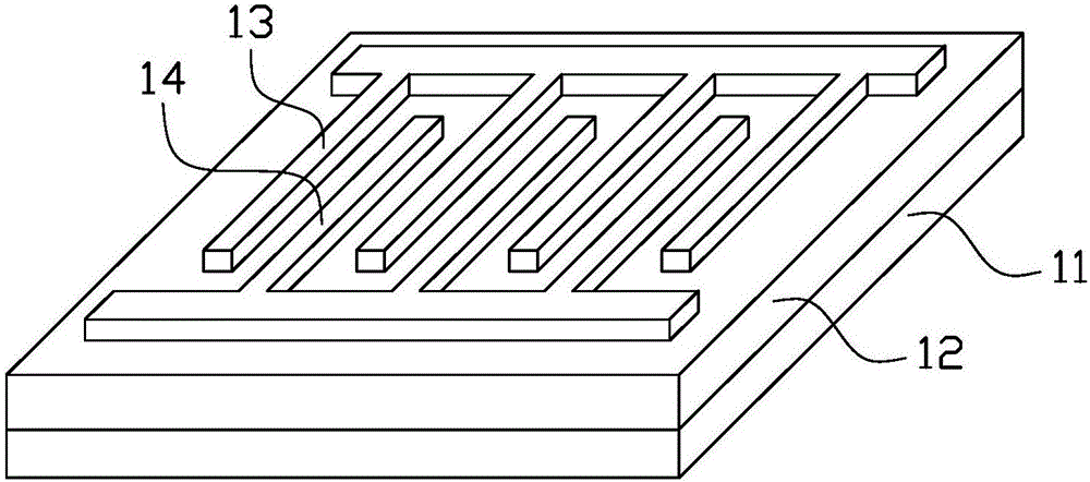
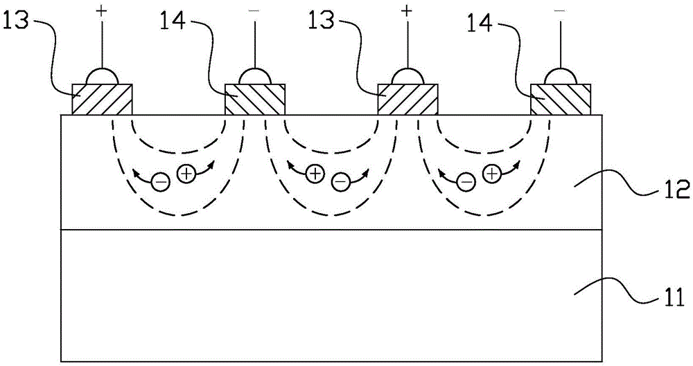
[0030] A light sensor with a metal-semiconductor-metal (Metal-Semiconductor-Metal, MSM) structure can convert light signals into current signals. like figure 1 and figure 2 As shown, a semiconductor layer 12 is formed on a substrate 11, and a pair of metal electrodes 13 and 14 are deposited on the semiconductor layer 12, that is, a photosensor with a metal-semiconductor-metal structure is formed. In the figure, the two metal electrodes 13 and 14 are interdigitated. When light of an appropriate wavelength is incident on the photosensor, the valence band electrons of the semiconductor layer 12 absorb photon energy and transition to the conduction band, and g...


PUM


Abstract

The invention provides a thin film transistor array substrate, a manufacturing method and a liquid crystal display panel. The thin film transistor array substrate comprises a substrate, scanning lines, data lines, signal input lines and current feedback lines, wherein the scanning lines, the data lines, the signal input lines and the current feedback lines are formed on the substrate. The scanning lines and the data lines intersect to define multiple sub-pixels. A thin film transistor, a light sensor and a pixel electrode are formed in each sub-pixel. Each thin film transistor comprises a first grid, a first semiconductor, a first source electrode and a first drain electrode. The first grids are connected with the scanning lines, the first source electrodes and the first drain electrodes are alternately arranged and both make contact with the first semiconductors, the first source electrodes are connected with the data lines, and the first drain electrodes are connected with the pixel electrodes. Each light sensor comprises a second grid, a second semiconductor, a second source electrode and a second drain electrode. The second grids do not receive signals, the second source electrodes and the second drain electrodes are alternately arranged and both make contact with the second semiconductors, the second source electrodes are connected with the signal input lines, and the second drain electrodes are connected with the current feedback lines.

Description

technical field [0001] The invention relates to the technical field of liquid crystal display, in particular to a thin film transistor array substrate and a manufacturing method, and a liquid crystal display panel with the thin film transistor array substrate. Background technique [0002] With the development of display technology, liquid crystal display panels (Liquid Crystal Display, LCD) are more and more popular due to their advantages of lightness and low radiation. The liquid crystal display panel includes a thin film transistor array substrate and a color filter substrate arranged oppositely, and a liquid crystal layer sandwiched between them. [0003] When the display panel is in different external environments, there will be more light components of a certain color in the external light, for example, more red light, and the normal display of the panel will be redder. In addition, short-wavelength light affects the retina of the human eye and can easily induce reti...

Claims


Application Information

Patent Timeline
Patent Type & Authority Applications(China)
IPC IPC(8): G02F1/1362G02F1/1368H01L27/12
CPCH01L27/1214H01L27/1259G02F1/136227G02F1/136286G02F1/1368G02F1/136295
Inventor 钟德镇陈尧
Owner KUSN INFOVISION OPTOELECTRONICS
Why Eureka
Try Eureka