Radio-frequency horizontal double diffusion metal oxide semiconductor device and manufacturing method

A technology of oxide semiconductor and fabrication method, applied in semiconductor/solid-state device manufacturing, semiconductor devices, electrical components, etc., can solve problems such as large size, existing risks, and the sinking area cannot be well connected to the source area.

Active Publication Date: 2016-12-07
FOUNDER MICROELECTRONICS INT
View PDF5 Cites 0 Cited by
  • Summary
  • Abstract
  • Description
  • Claims
  • Application Information

AI Technical Summary

Problems solved by technology

The disadvantage of this method is that the silicon etch of the sinker layer creates a groove in the silicon surface, which is fractured in the implanted area during the subsequent implantation, e.g. figure 1 As shown in , it can be seen that there is a cross-section in the shaded part, which makes the sinking region not well connected to the source region. Although the sinking ion drive will reduce the influence of the cross-section, there is still a risk
This risk makes the on-resistance of the device unstable and tends to be large

Method used


Image

  • Radio-frequency horizontal double diffusion metal oxide semiconductor device and manufacturing method
  • Radio-frequency horizontal double diffusion metal oxide semiconductor device and manufacturing method
  • Radio-frequency horizontal double diffusion metal oxide semiconductor device and manufacturing method

Examples


Embodiment Construction

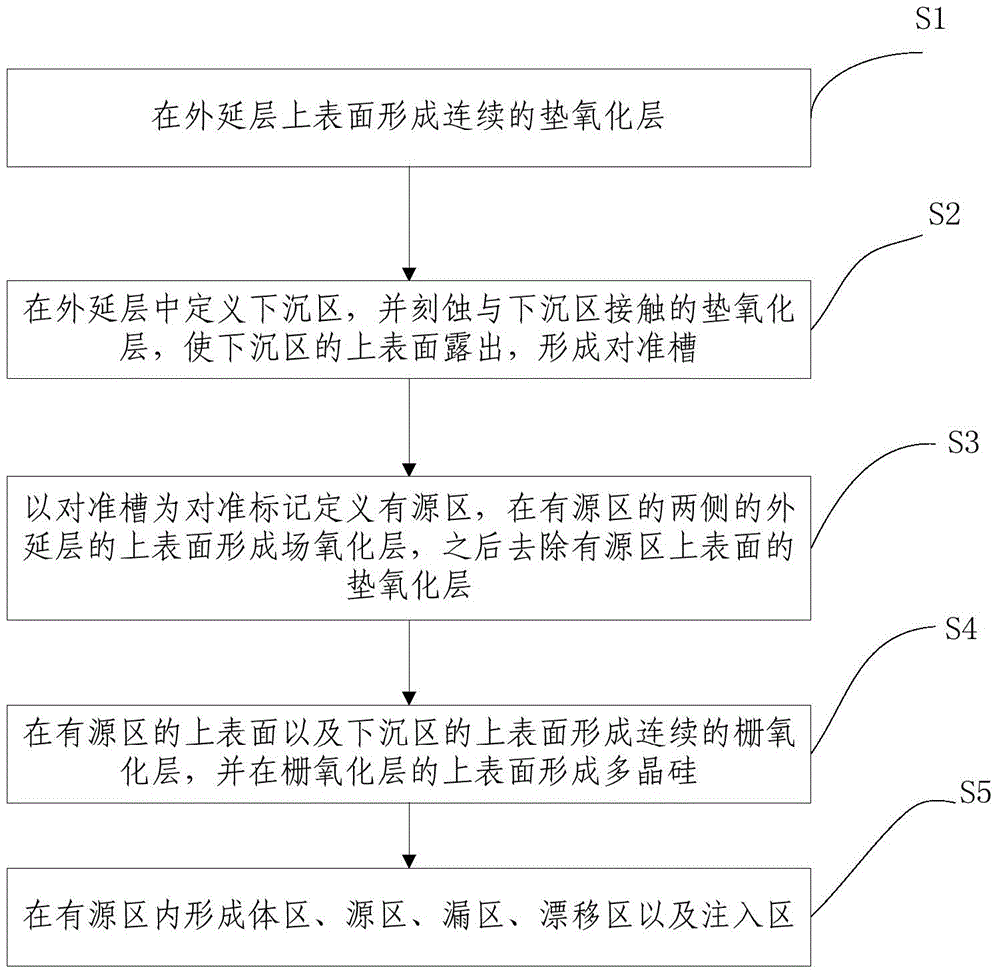
[0041] The present invention will be described in further detail below in conjunction with the accompanying drawings and embodiments. The following examples are used to illustrate the present invention, but should not be used to limit the scope of the present invention.

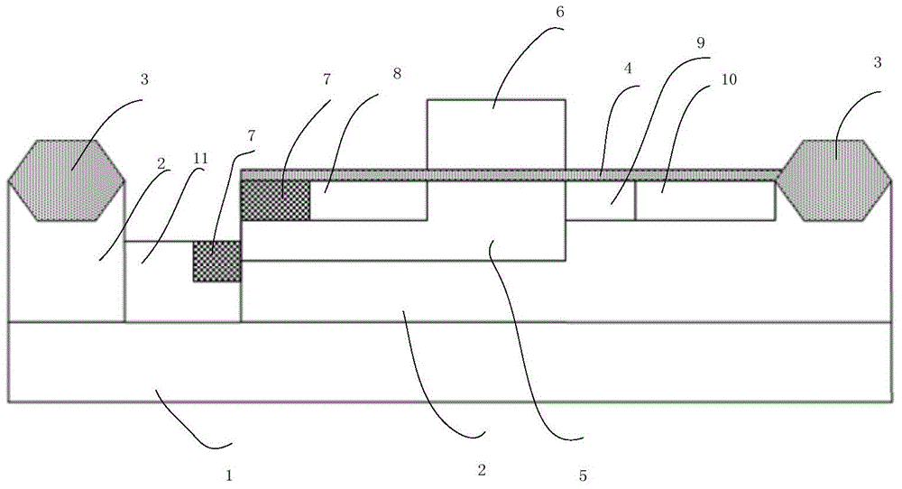
[0042] figure 1 It is a schematic diagram of the structure of a radio frequency horizontal double-diffused metal oxide semiconductor device in the prior art. It can be seen from the figure that the device includes a substrate 1, an epitaxial layer 2, a field oxide layer 3, a gate oxide layer 4, a body region 5, and a polysilicon 6. Implantation region 7 , source region 8 , drift region 9 , drain region 10 and sinker region 11 . The implantation region 7 connects the sinker region 11 to the source region 8, and the implantation region 7 and the source region 8 are short-circuited through the metal of the contact hole. After the channel under the polysilicon is formed, the current can flow from the drain regi...


PUM

PropertyMeasurementUnit
Thicknessaaaaaaaaaa
Thicknessaaaaaaaaaa
Thicknessaaaaaaaaaa

Abstract

The invention discloses a radio-frequency horizontal double diffusion metal oxide semiconductor device and a manufacturing method thereof. An alignment mark of a subsidence region is formed by employing a pad oxide layer etching method, so as to define an active region. The method is simple in process, the maneuverability is high, and meanwhile, the condition that a fracture surface exists in an injection region due to a groove formed through silicon etching in the prior art is avoided, so that the injection region can be better connected with the subsidence region; and the on resistance of the device is effectively reduced. Furthermore, due to the absence of silicon etching, the lattice defect easily generated in silicon etching is also avoided.

Description

technical field [0001] The invention relates to the field of semiconductor chip manufacturing, and more specifically relates to a radio frequency horizontal double-diffusion metal oxide semiconductor device and a manufacturing method thereof. Background technique [0002] Radio frequency horizontal double-diffused metal oxide semiconductor (RF LDMOS) is widely used in mobile phone base stations, broadcast television and radar and other fields. The process of RF LDMOS generally includes sinker layer, polysilicon, body region layer, source and drain layer, injection layer and so on. The working principle of the RF LDMOS device is that the implantation region connects the sinker region to the source region, and the implantation region and the source region are short-circuited through the metal of the contact hole. After the channel under the polysilicon is formed, the current can flow from the drain region to the source region, then flow through the metal in the contact hole t...

Claims


Application Information

Patent Timeline
IPC IPC(8): H01L29/78H01L29/06H01L21/336H01L21/265
Inventor 闻正锋邱海亮马万里赵文魁
Owner FOUNDER MICROELECTRONICS INT
Why Eureka
Try Eureka