Solar cell piece array, solar cell module and preparation method therefor
A technology for solar cells and solar cells, applied in the field of solar cells, can solve the problems of small conductive cross-sectional area and large resistance loss, and achieve the effects of reducing the number of metal wires, low cost, and simple preparation
- Summary
- Abstract
- Description
- Claims
- Application Information
AI Technical Summary
Problems solved by technology
Method used
Image
Examples
preparation example Construction
[0117] During the preparation process of the solar cell module 100 , the conductive wire can be welded to the auxiliary grid line and the back electrode of the battery sheet 31 first, and then the various layers are stacked and laminated.
[0118] Other components of the solar cell assembly 100 according to the present application may be known in the art, and will not be repeated here.
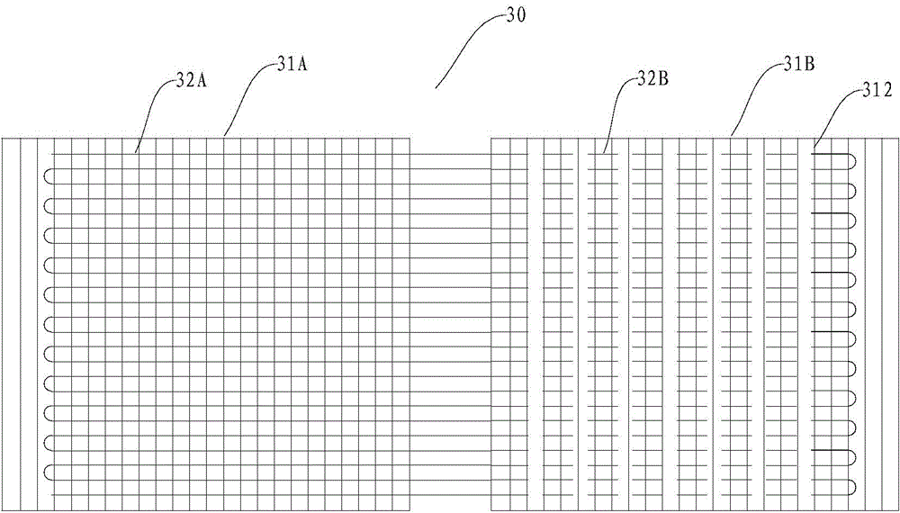
[0119] Specifically, the solar cell module 100 includes an upper cover plate 10 , a front adhesive film layer 20 , a cell array 30 , a rear adhesive film layer 40 and a back sheet 50 . The battery sheet array 30 includes a plurality of battery sheets 31 , adjacent battery sheets 31 are connected by a plurality of conductive wires 32 , and the front adhesive film layer 20 is in direct contact with the conductive wires 32 and filled between the adjacent conductive wires 32 .
[0120] In other words, the solar cell assembly 100 according to the embodiment of the present application includes a top...
example 1
[0144] Example 1 is used to illustrate an example of the solar cell module 100 of the present application and its manufacturing method.
[0145] (1) Preparation of wire S
[0146] Attach a layer of Sn40%-Bi55%-Pb5% alloy layer (melting point is 125 ℃) on the surface of the copper wire, wherein the cross-sectional area of the copper wire is 0.04mm 2 , the thickness of the alloy layer is 16 μm, thereby making a wire S.
[0147] (2) Preparation of solar cell module 100
[0148] Provide a POE film layer with a size of 1630×980×0.5mm (melting temperature is 65°C), and accordingly provide a glass plate with a size of 1633×985×3mm and 60 pieces of polycrystalline silicon cells with a size of 156×156×0.21mm Tablet 31. The battery sheet 31 has 91 auxiliary grid lines (made of silver, with a width of 60 microns and a thickness of 9 microns), each auxiliary grid line basically runs through the battery sheet 31 in the longitudinal direction, and the distance between adjacent auxiliar...
example 2
[0156] Example 2 is used to illustrate an example of the solar cell module of the present application and its preparation method.
[0157] (1) Preparation of conductive wire
[0158] Attach a layer of Sn40%-Bi55%-Pb5% alloy layer (melting point is about 125°C) on the surface of the copper wire, wherein the cross-sectional area of the copper wire is 0.03mm 2 , the thickness of the alloy layer is 10 micrometers, thereby making a conductive wire.
[0159] (2) Preparation of solar cell modules
[0160] Provide an EVA film layer with a size of 1630×980×0.5mm (melting temperature is 60°C), a glass plate with a size of 1633×985×3mm and 60 pieces of polycrystalline silicon cells 31 with a size of 156×156×0.21mm. The light-receiving surface of the battery sheet 31 is provided with 91 auxiliary grid lines (the material is silver, the width is 60 microns, and the thickness is 9 microns), and each auxiliary grid line basically runs through the battery sheet 31 in the longitudinal direct...
PUM
 Abstract
Description
Claims
Application Information


