Low power consumption dynamic threshold comparator interface circuit and rectifier, wireless sensor
A comparator circuit and dynamic threshold technology, applied in the direction of logic circuit interface device, logic circuit connection/interface layout, etc., can solve the problems of wireless sensors such as small size, limited battery energy, and inability to meet long-term work needs, and eliminate oscillation phenomenon , low working voltage and simple structure
- Summary
- Abstract
- Description
- Claims
- Application Information
AI Technical Summary
Problems solved by technology
Method used
Image
Examples
Embodiment 1
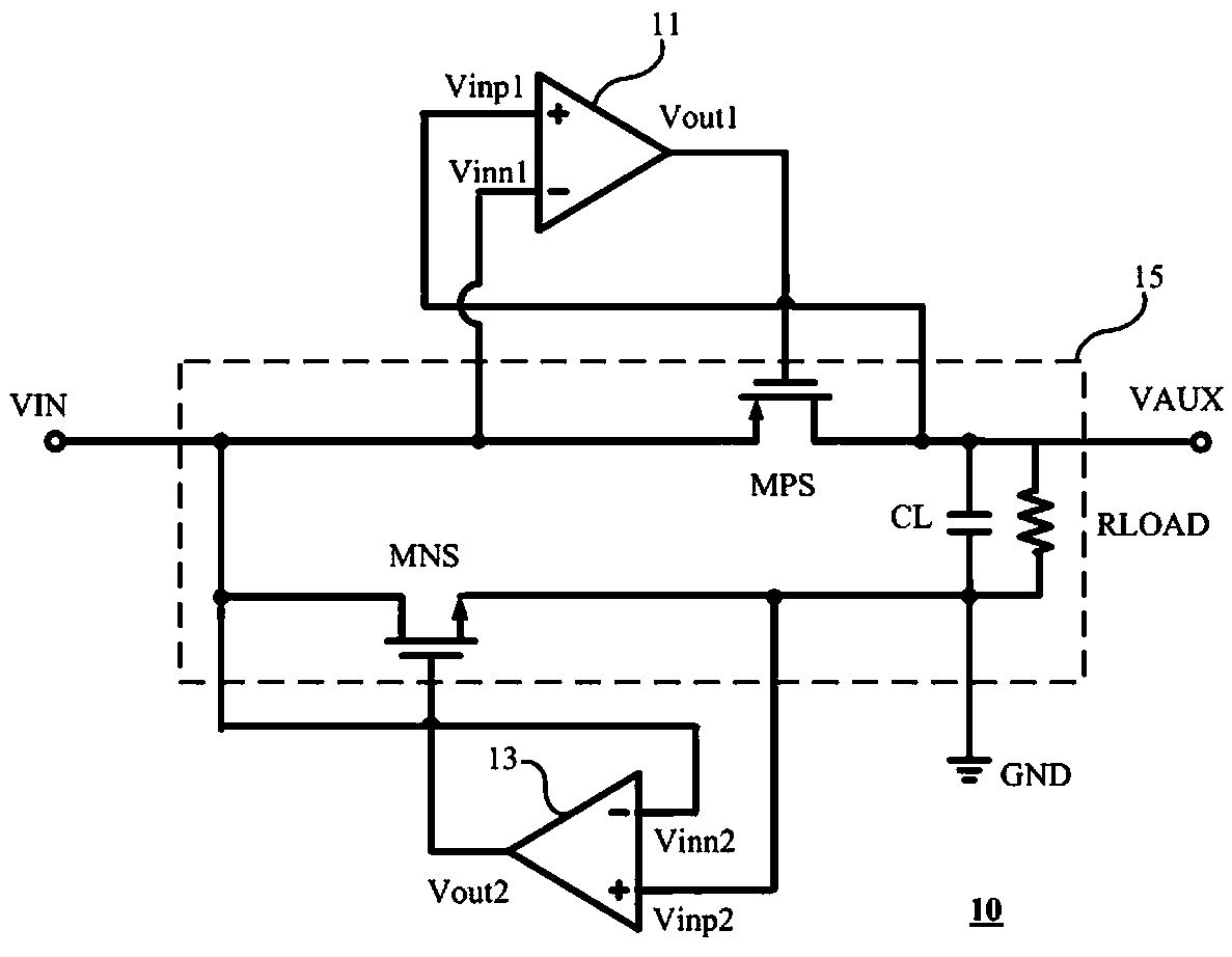
[0035] See figure 1 and Figure 4 , figure 1 It is a schematic circuit structure diagram of a low-power dynamic threshold comparator interface circuit provided by an embodiment of the present invention; Figure 4 It is a schematic diagram of a circuit structure of a switching load circuit provided by an embodiment of the present invention. The low power consumption dynamic threshold comparator interface circuit 10 includes: an input terminal VIN, an output terminal VAUX, a first comparator circuit 11, a second comparator circuit 13, a switch load circuit 15 and a ground terminal GND; wherein the switch The load circuit 15 includes a first power switch MPS, a second power switch MNS, a load capacitor CL, and a load resistor RLOAD. The first power switch MPS is electrically connected between the input terminal VIN and the output terminal VAUX and controls terminal is electrically connected to the output terminal Vout1 of the first comparator circuit 11, the load capacitance C...
Embodiment 2
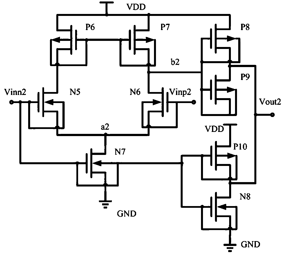
[0045] see again Figure 1 to Figure 4 , this embodiment describes in detail the low power consumption dynamic threshold comparator interface circuit 10 of the present invention on the basis of the above embodiments. details as follows:
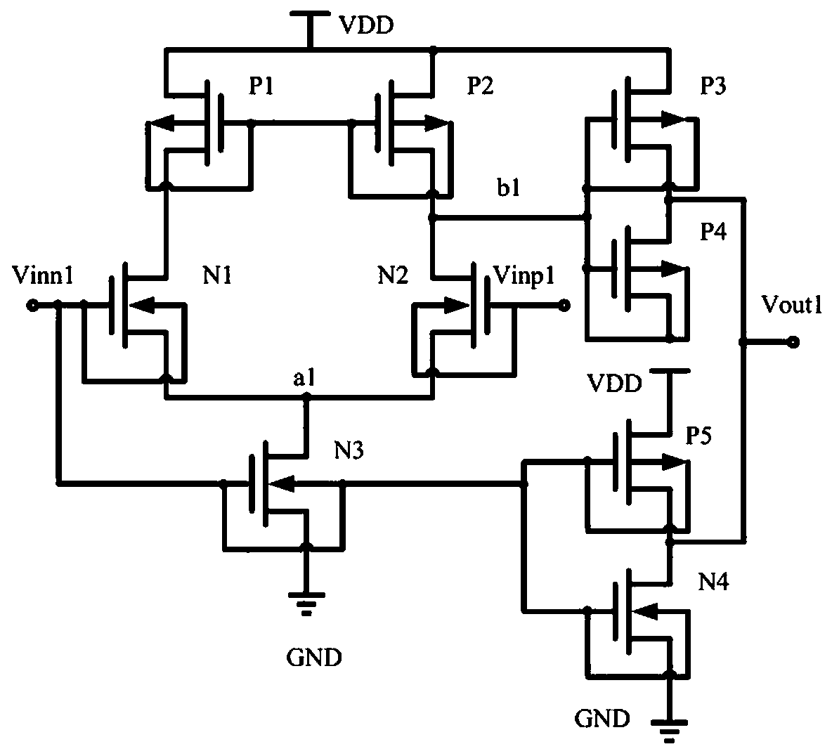
[0046] 1. The dynamic threshold comparator 1 is the first comparator circuit 11
[0047] See figure 2 , mainly composed of five PMOS transistors P1, P2, P3, P4, and P5 and four NMOS transistors N1, N2, N3, and N4.
[0048] The source terminal of P1 is connected to the power supply voltage VDD, the drain terminal of P1 is connected to the drain terminal of N1, the gate terminal of P1 is connected to the substrate of P1, the gate terminal of P2, and the substrate of P2, and the substrate of P1 is connected to the gate terminal of P1 The gate terminal of P2 is connected to the substrate of P2;
[0049] The source terminal of P2 is connected to the power supply voltage VDD, the drain terminal of P2 is connected to the drain terminal of N2, t...
Embodiment 3
[0081] The invention also provides a rectifier and a wireless sensor. The building blocks of the wireless sensor are housed in a housing, which includes a rectifier. The rectifier is a rectifying device whose main function is to change alternating current (AC) into direct current (DC), and after filtering, charge energy storage elements such as supercapacitors or rechargeable batteries for use by loads. For the rectifier of the present invention, it can include The low power consumption dynamic threshold comparator interface circuit 10 in the above embodiments.
PUM
 Abstract
Description
Claims
Application Information


