Substrate for micro electro mechanical system chip, micro electro mechanical system chip and preparation method thereof

A micro-electro-mechanical system and substrate technology, applied in the field of micro-mechanics, can solve the problems of low efficiency and large chip size, and achieve the effect of cost-effective, complex structure, and 3D chip stacking

Inactive Publication Date: 2017-01-04
苏州工业园区纳米产业技术研究院有限公司
View PDF9 Cites 4 Cited by
  • Summary
  • Abstract
  • Description
  • Claims
  • Application Information

AI Technical Summary

Problems solved by technology

However, this process also has certain limitations. Generally, the etching angle is relatively vertical (by this etching method, a cavity 1 is formed at one time, and the cavity wall of the cavity 1 is a vertical surface 11, such as Figure 1a ), or form an inverted trapezoidal shape with the bottom slightly larger than the top (by this etching method, an inverted trapezoidal cavity 2 is formed at one time, and the cavity wall 21 of the cavity 2 is a slope, such as 1b), or the top is slightly larger than the bottom trapezoidal shape (by this etching method, a positive trapezoidal cavity 3 is formed at one time, and the cavity wall 31 of the cavity 3 is a slope, such as 1c)
In addition, the use efficiency of this structure is low, and the volume of the formed chip is relatively large.

Method used


Image

  • Substrate for micro electro mechanical system chip, micro electro mechanical system chip and preparation method thereof
  • Substrate for micro electro mechanical system chip, micro electro mechanical system chip and preparation method thereof
  • Substrate for micro electro mechanical system chip, micro electro mechanical system chip and preparation method thereof

Examples


Embodiment Construction

[0035] The specific implementation manners of the present invention will be further described in detail below in conjunction with the accompanying drawings and embodiments. The following examples are used to illustrate the present invention, but are not intended to limit the scope of the present invention.

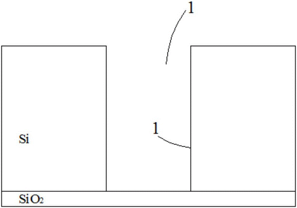
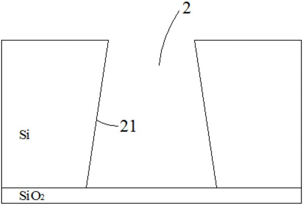
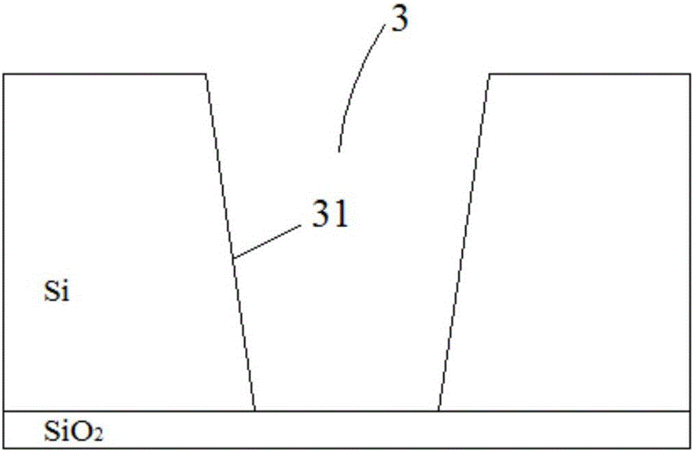
[0036] The micro-electro-mechanical system chip of the present invention includes a substrate for the micro-electro-mechanical system chip, see figure 2 A substrate 40 for MEMS chips shown in a preferred embodiment of the present invention includes a substrate body 41 having an upper surface 41a and a lower surface 41b and at least one formed in the substrate body 41 Cavity 42 . Each cavity 42 includes an upper sub-cavity 421 and a lower sub-cavity 422 arranged up and down. The upper surface 41 a of 41 extends downward, and the shape surrounded by the upper sub-cavity 421 is different from the shape surrounded by the lower sub-cavity 422 . On the lower surface 41 b of ...


PUM


Abstract

The invention relates to a substrate for a micro electro mechanical system chip, the micro electro mechanical system chip and a preparation method thereof, and belongs to the field of micromechanics. The substrate for the micro electro mechanical system chip comprises a substrate body and at least one cavity, wherein the substrate body has the upper surface and the lower surface; the at least one cavity is formed in the substrate body; each cavity comprises an upper sub cavity part and a lower sub cavity part in vertical arrangement; the upper sub cavity part and the lower sub cavity part are communicated; the upper sub cavity is formed by downwards extending from the upper surface of the substrate body; the shape and / or the dimension defined by the upper sub cavity part are / is different from the shape and / or the dimension defined by the lower sub cavity part; the positive projection area of the upper sub cavity part is greater than the positive projection area of the lower sub cavity part on the lower surface of the substrate body.

Description

technical field [0001] The invention relates to a substrate for a micro-electromechanical system chip, a micro-electromechanical system chip and a preparation method for the substrate, belonging to the field of micromechanics. Background technique [0002] Micro-Electro-Mechanical Systems (MEMS, Micro-Electro-Mechanical System), also known as micro-electro-mechanical systems, micro-systems, micro-machines, etc., are developed on the basis of microelectronics technology (semiconductor manufacturing technology), integrating lithography, corrosion , thin film, LIGA, silicon micromachining, non-silicon micromachining and precision machining technologies to produce high-tech electromechanical devices. [0003] With the rapid development of the semiconductor industry, through-silicon via etching technology is becoming more and more important, especially in the fields of 3D packaging and MEMS, bulk silicon etching is an essential key step. At present, in the field of through-silic...

Claims


Application Information

Patent Timeline
Patent Type & Authority Applications(China)
IPC IPC(8): B81B1/00B81C1/00
CPCB81B1/002B81C1/00087
Inventor 李全宝
Owner 苏州工业园区纳米产业技术研究院有限公司
Why Eureka
Try Eureka