MPS diode and manufacturing method therefor

A technology of diode and ion implantation area, which is applied in semiconductor/solid-state device manufacturing, electrical components, electric solid-state devices, etc. It can solve the problems of increasing device leakage risk, device surface damage, and implantation dose should not be too small, so as to ensure ohmic contact quality, improved performance, and reduced leakage current effects

Inactive Publication Date: 2017-01-04
PEKING UNIV FOUNDER GRP CO LTD +1
View PDF4 Cites 7 Cited by
  • Summary
  • Abstract
  • Description
  • Claims
  • Application Information

AI Technical Summary

Problems solved by technology

[0004] Existing MPS diodes are implanted only once during manufacture. In order to ensure a good ohmic contact, the implant dose should not be too small, but a large dose injected once will cause certain damage to the device surface and increase the risk of leakage of the device.

Method used


Image

  • MPS diode and manufacturing method therefor
  • MPS diode and manufacturing method therefor
  • MPS diode and manufacturing method therefor

Examples


Embodiment Construction

[0038] Embodiments of the present invention will be described in detail below with reference to the accompanying drawings.

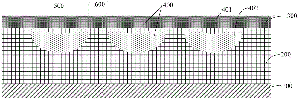
[0039] The MPS diode is a device structure that can be designed to exhibit the low turn-on voltage of a Schottky diode in the forward direction and the low reverse leakage current of a P-i-N diode in the reverse direction. MPS diodes may include Schottky contacts with one or more buried p-n junctions (or P-i-N regions) in the area of ​​the contacts. The forward conduction voltage is controlled by the Schottky section before the p-n junction conducts at a higher voltage. The reverse mode of operation is controlled through appropriately spaced p-n junctions. Furthermore, in some embodiments, the same process used to form the p-n junction buried within the region of the Schottky contact can also be used to form the edge termination structure to provide an edge termination for the MPS diode.

[0040] figure 1 A schematic cross-sectional view of the MPS di...


PUM


Abstract

The invention relates to an MPS diode and a manufacturing method therefor. The MPS diode comprises a substrate, and an epitaxial layer and a metal layer which are arranged on the substrate in sequence, wherein the diode also comprises multiple ion implantation regions which are embedded in the epitaxial layer and are in contact with the metal layer; the ion implantation regions are formed by implanting doped ions in the epitaxial layer; each ion implantation region comprises a first ion implantation region and a second ion implantation region; the second ion implantation region is embedded in the first ion implantation region; and in addition, the upper surface of the first ion implantation region and the upper surface of the second ion implantation region are both in contact with the metal layer. According to the MPS diode and the manufacturing method therefor, through the multiple times of ion implantation, the leakage current of a device is lowered; the on-state voltage drop of the device is lowered; and the performance of the device is improved.

Description

technical field [0001] The invention relates to the technical field of semiconductor chip manufacturing technology, in particular to an MPS (mixed PIN and Schottky) diode and a manufacturing method thereof. Background technique [0002] Power diodes are key components of circuit systems, and are widely used in high-frequency inverters, digital products, generators, televisions and other civilian products, as well as satellite receivers, missiles and aircraft and other advanced weapon control systems and instrumentation equipment. Military occasions. Power diodes are expanding in two important directions: (1) to tens of millions or even tens of thousands of amperes, which can be applied to high-temperature arc wind tunnels, resistance welding machines, etc.; (2) reverse recovery time is getting shorter and shorter, showing Developing in the direction of ultra-fast, ultra-soft, and ultra-durable, it is not only used in rectification occasions, but also has different functions...

Claims


Application Information

Patent Timeline
Patent Type & Authority Applications(China)
IPC IPC(8): H01L27/08H01L21/266
Inventor 李理马万里赵圣哲姜春亮
Owner PEKING UNIV FOUNDER GRP CO LTD
Why Eureka
Try Eureka