
AMOLED panel and preparation method thereof

A panel and substrate technology, which is applied in the field of AMOLED panels and the preparation of the AMOLED panels, can solve the problems of not being able to highlight the light and thin characteristics of AMOLED panels, increase materials, and increase costs, so as to improve bending resistance, increase strength, and strengthen strength Effect

Active Publication Date: 2017-01-04
EVERDISPLAY OPTRONICS (SHANGHAI) CO LTD
View PDF3 Cites 6 Cited by
  • Summary
  • Abstract
  • Description
  • Claims
  • Application Information

AI Technical Summary

Problems solved by technology

This method also cannot highlight the thin and light characteristics of the AMOLED panel, and additional materials are used, which increases the cost

Method used


Image

  • AMOLED panel and preparation method thereof
  • AMOLED panel and preparation method thereof
  • AMOLED panel and preparation method thereof

Examples


Embodiment Construction

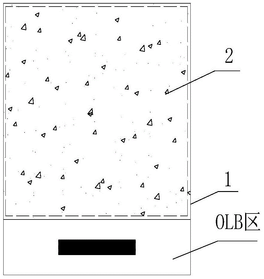
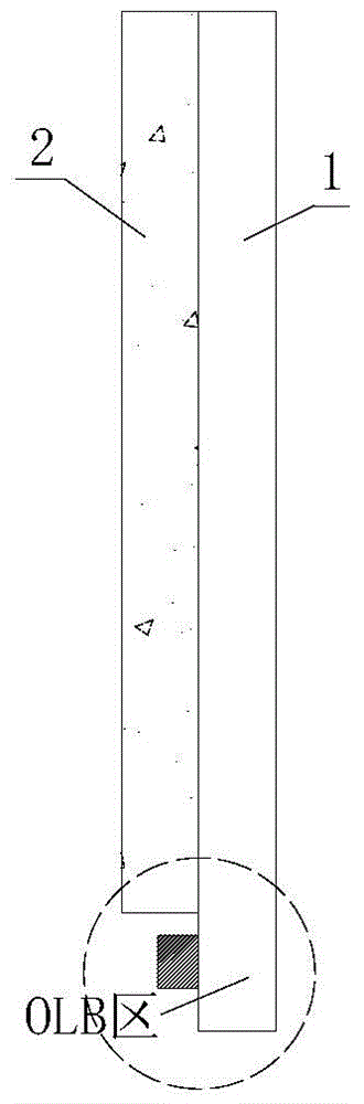
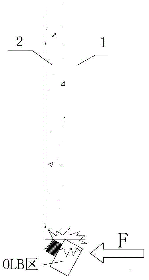
[0056]The AMOLED panel provided in the embodiment of the present invention, such as Figure 3a As shown in and 3 b , it includes a substrate glass 1 and a cover glass 2 fixedly arranged on the substrate glass 1 . The substrate glass 1 is provided with an OLB area and an active matrix area. In the embodiment of the present invention, the cover glass 2 only covers the active matrix area, not the OLB area. Since the cover glass 2 covers the active matrix area, the active matrix area is not marked in the following description and drawings, but this is not a limitation of the present invention. Wherein, the OLB area includes a device area 11 (including an integrated circuit area (IC area), a flexible circuit board area (FPC area) and a test point area (Test PAD area)) and a non-device area 12, and the non-device area 12 is covered with Reinforcement film6. The non-device area 12 is preferably located at the sharp corner of the substrate glass 1 and surrounds the device area 12, s...


PUM


Abstract

The invention relates to the field of semiconductor device manufacture, and particularly to an AMOLED panel and a preparation method thereof. Through spray-printing of materials with relatively high strength, such as a high-molecular material or metal powder, into a non-device area of a substrate glass OLB area by means of 3D printing technology on the non-device area in the OLB area of the AMOLED panel, a reinforcing film is formed. Furthermore the thickness of the reinforcing film is not larger than that of cover plate glass which covers the substrate glass. Furthermore under a precondition that integral thin performance of the AMOLED panel is kept, bending resistance of the whole OLB area on the AMOLED panel can be effectively improved just through adding reinforcing structures such as the reinforcing film in the non-device area, and probability of defects such as a corner collapse fragment in a device is greatly reduced.

Description

technical field [0001] The invention relates to the field of semiconductor device manufacturing, in particular to an AMOLED panel and a preparation method of the AMOLED panel. Background technique [0002] The display unit of the AMOLED (Active Matrix Organic Light Emitting Diode) panel is composed of substrate glass (LTPS TFT Glass) and cover glass (Encap Glass). , COG is the abbreviation of chip onglass, that is, the area on which the chip is bound on the substrate glass) is a single glass plate. Such as Figure 1a and Figure 1b As shown, there is only one layer of substrate glass in the OLB area. The dotted box represents the active matrix area. When the thickness of the substrate glass is as thin as 0.3 mm or even 0.2 mm, the corners of the single glass plate area are prone to chipping and chipping due to external forces during system assembly or use, resulting in malfunctions. Such as Figure 1c As shown, when the external force F acts on the OLB area, it is easy ...

Claims


Application Information

Patent Timeline
IPC IPC(8): H01L27/32H01L51/52H01L51/56
Inventor 唐志舜
Owner EVERDISPLAY OPTRONICS (SHANGHAI) CO LTD
Learn More