Epitaxial growth method and epitaxial layer with heterostructure buried

An epitaxial growth and epitaxial structure technology, applied in laser parts, electrical components, lasers, etc., can solve problems such as threshold current and low optical power, and achieve the effect of reducing threshold current density, reducing Auger recombination, and improving high temperature characteristics

Active Publication Date: 2017-01-04
WUHAN HUAGONG GENUINE OPTICS TECH
View PDF3 Cites 5 Cited by
  • Summary
  • Abstract
  • Description
  • Claims
  • Application Information

AI Technical Summary

Problems solved by technology

Because BH (buried heterostructure) technology can more effectively confine the carriers in the epitaxial layer, it can make the threshold current of the laser lower and the optical power higher. However, AlGaInAs is easily oxidized, which limits its application in BH. At present, All related major companies are researching the BH technology of AlGaInAs

Method used


Image

  • Epitaxial growth method and epitaxial layer with heterostructure buried
  • Epitaxial growth method and epitaxial layer with heterostructure buried
  • Epitaxial growth method and epitaxial layer with heterostructure buried

Examples


Embodiment Construction

[0024] An epitaxial growth method and an epitaxial layer for burying a heterostructure according to the present invention will be further described below in conjunction with the accompanying drawings and embodiments.

[0025] The following is a best example of an epitaxial growth method and an epitaxial layer buried in a heterostructure described in the present invention, which does not limit the protection scope of the present invention.

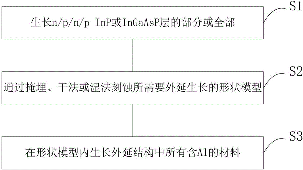
[0026] figure 1 An epitaxial growth method is shown, comprising the following steps:

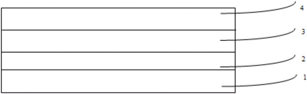
[0027] S1, growing part or all of the n / p / n / p InP or InGaAsP layer;

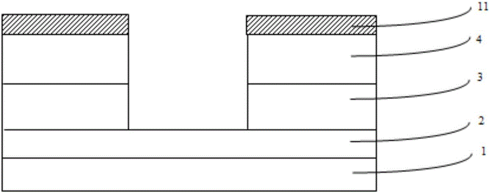
[0028] S2, the shape model of epitaxial growth required by burial, dry or wet etching;

[0029] S3. Growing all Al-containing materials in the epitaxial structure in the shape model.

[0030] Preferably, the step S1 specifically includes growing a Buffer layer, a first p-InP layer, and an n-InP layer sequentially on an InP substrate; the Buffer layer is an n-type InP buffer layer.

...


PUM


Abstract

The invention relates to an epitaxial growth method and an epitaxial layer with a heterostructure buried. The epitaxial growth method includes following steps: S1, growing part of or all of an n / p / n / p InP or InGaAsP layer; S2, etching a shape model needing epitaxial growth through burying, a dry method or a wet method; S3, growing all material containing Al in an epitaxial structure in the shape model. Part of or all of an n / p / n / p structure is formed, the shape of the epitaxial layer needing growth is etched, and the epitaxial layer is grown in the shape. By utilizing the method, the advantages of AlGaInAs / InP materials and BH technology can be combined effectively to grow an efficient laser device epitaxial structure, effects of avoiding Al oxidation, lowering auger recombination and interband adsorption and improving high-temperature characteristics of devices are realized, threshold current density of a laser device is reduced, and feature temperature of an active layer material and external quantum efficiency, internal quantum efficiency and conversion efficiency of an active area quantum well are increased.

Description

technical field [0001] The invention relates to the field of semiconductor lasers, in particular to an epitaxial growth method and an epitaxial layer for burying heterostructures. Background technique [0002] The semiconductor laser has developed from the initial operation at low temperature of 25°C to continuous operation at room temperature, and now it has developed to continuous operation at high temperature of 85°C. The active region of the semiconductor laser has developed from a homojunction to a single heterojunction, a double heterojunction, and a quantum well. (Single, multiple quantum wells) and other forms, in the final analysis, improve the external quantum efficiency, internal quantum efficiency and conversion efficiency of the semiconductor active layer material. [0003] In the prior art, the conduction band offset ΔEc=0.72ΔEg in the quantum well structure of AlGaInAs / InP material has a larger electron confinement potential than InGaAsP / InP (ΔEc=0.4ΔEg), whic...

Claims


Application Information

Patent Timeline
Patent Type & Authority Applications(China)
IPC IPC(8): H01S5/323H01L21/02
CPCH01L21/02365H01L21/02538H01L21/02543H01L21/02546H01S5/323
Inventor 李鸿建
Owner WUHAN HUAGONG GENUINE OPTICS TECH
Why Eureka
Try Eureka