Preparation method and product of high-performance metal grid transparent conductive film

A technology of transparent conductive film and metal mesh, applied in metal/alloy conductor, cable/conductor manufacturing, conductive layer on insulating carrier, etc., which can solve the problems of inflexibility and visible metal mesh.

Active Publication Date: 2017-02-01
BEIJING HINANO TECH CO LTD
View PDF4 Cites 14 Cited by
  • Summary
  • Abstract
  • Description
  • Claims
  • Application Information

AI Technical Summary

Problems solved by technology

[0003] In order to solve the above technical problems, especially to solve the problems of non-bendability and visible metal grid, the present invention proposes a high-performance metal grid transparent conductive film and its preparation method

Method used


Image

  • Preparation method and product of high-performance metal grid transparent conductive film
  • Preparation method and product of high-performance metal grid transparent conductive film
  • Preparation method and product of high-performance metal grid transparent conductive film

Examples


Embodiment 1

[0058] The metal grid transparent conductive thin film structure of this embodiment is as Figure 7 (a), where,

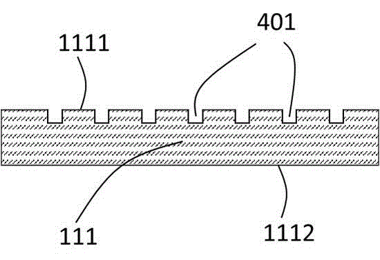
[0059] 105 is a PET transparent substrate with a thickness of 125 microns, 1051 is the first surface of the PET transparent substrate, and 1052 is the second surface of the PET transparent substrate;

[0060] 301 is a groove layer, the material of the groove layer is UV curable glue, and its thickness is 20 microns, and the groove layer 301 is located on the first surface 1051 of the PET transparent substrate;

[0061] 206 is a metal grid wiring, and the metal grid wiring is formed by close contact between graphene and metal nanoparticles grown on it in situ, and its structural schematic diagram is as follows Figure 4 shown. The metal mesh wiring 206 is completely contained within the surface of the groove layer 301 .

[0062] The specific preparation method is as follows:

[0063] S1, providing a PET transparent substrate comprising a first surface and a seco...

Embodiment 2

[0073] The metal grid transparent conductive thin film structure of this embodiment is as Figure 7 (a), where,

[0074] 105 is a PET transparent substrate with a thickness of 125 microns, 1051 is the first surface of the PET transparent substrate, and 1052 is the second surface of the PET transparent substrate;

[0075] 301 is a groove layer, the material of the groove layer is UV curable glue, and its thickness is 20 microns, and the groove layer 301 is located on the first surface 1051 of the PET transparent substrate;

[0076] 206 is a metal grid grid wiring, and the metal grid wiring is formed by close contact between graphene and gold nanoparticles grown on it in situ, and its structural schematic diagram is as follows Figure 4 As shown, the average diameter of the gold nanoparticles is 20 nm, and the average size of the graphene is 500 nm. The metal mesh wiring 206 is completely contained within the surface of the groove layer 301 .

[0077] The specific preparation...

Embodiment 3

[0082] The metal grid transparent conductive thin film structure of this embodiment is as Figure 7 (d), where:

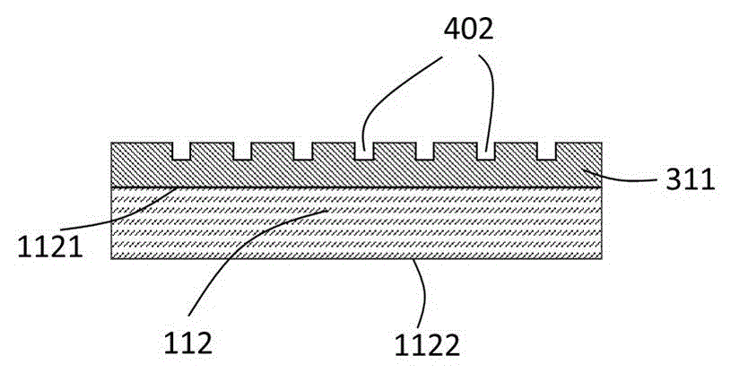
[0083] 108 is a PET transparent substrate with a thickness of 125 microns, 1081 is the first surface of the PET transparent substrate, and 1082 is the second surface of the PET transparent substrate;

[0084] 304 is the first groove layer, 305 is the second groove layer, the material of the first groove layer and the second groove layer is UV curing glue, and its thickness is 20 microns, and the groove layer 304 is located on the PET transparent lining. above the bottom first surface 1081;

[0085] 209 is the first metal grid wiring, which is formed by close contact between the graphene and the metal nanoparticles grown on it in situ, and its structural schematic diagram is as follows Image 6 As shown, the first metal grid wiring 209 is completely contained within the surface of the first groove layer 304;

[0086] 210 is the second metal grid wiring, which is ...


PUM

PropertyMeasurementUnit
widthaaaaaaaaaa
diameteraaaaaaaaaa
sizeaaaaaaaaaa

Abstract

The invention provides a preparation method and product of a high-performance metal grid transparent conductive film. The metal grid transparent conductive film at least comprises a transparent substrate comprising a first surface and a second surface in opposite arrangement; and a metal grid wire formed by close contact between graphene and metal nanometer particles in-situ growing thereon, wherein the metal grid wire is directly or/and indirectly arranged on the first surface or/and the second surface of the transparent substrate. The prepared metal grid solves the problems of unbendable conventional metal grids, visible metal grids, metal migration and the like. The preparation method is simple, thereby facilitating large-scale production.

Description

technical field [0001] The invention relates to a method for preparing a metal grid transparent conductive film and its products, in particular to a method for preparing a high-performance metal grid transparent conductive film with ultra-fine line width, bendability and good stability and its product. Background technique [0002] There are various methods for preparing metal grids by printing techniques, and conventional techniques include: nanoimprinting, screen printing, inkjet printing, etc. Among them, the metal mesh prepared by nanoimprint technology has the highest precision, and its line width is usually 5 microns, which is suitable for some touch products, especially some large-size touch products. However, in mobile phones or tablet products, the metal grid is required to be invisible to the naked eye, and its line width must be at least less than 2 microns. Nanoimprinting technology can reduce the line width of embossed grooves to less than 2 microns, but there ...

Claims


Application Information

Patent Timeline
Patent Type & Authority Applications(China)
IPC IPC(8): H01B13/00H01B5/14H01B5/00H01B1/02H01B1/04B82Y30/00B82Y40/00
Inventor 刘腾蛟李丽坤范江峰谢丽萍任晓倩
Owner BEIJING HINANO TECH CO LTD
Why Eureka
Try Eureka