Semiconductor structure forming method

A technology of semiconductor and pseudo-gate structure, applied in semiconductor devices, semiconductor/solid-state device manufacturing, transistors, etc., can solve problems such as increasing the difficulty of manufacturing high-K metal gate transistors, shrinking, and performance degradation of high-K metal gate transistors

Active Publication Date: 2017-02-01
SEMICON MFG INT (SHANGHAI) CORP +1
View PDF5 Cites 16 Cited by
  • Summary
  • Abstract
  • Description
  • Claims
  • Application Information

AI Technical Summary

Problems solved by technology

[0005] However, as the size of semiconductor devices shrinks, the size of the high-K metal-gate transistor is also reduced accordingly, which increa

Method used


Image

  • Semiconductor structure forming method
  • Semiconductor structure forming method
  • Semiconductor structure forming method

Examples


Embodiment Construction

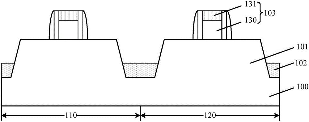
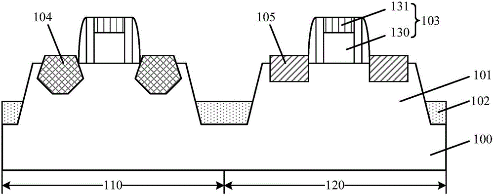
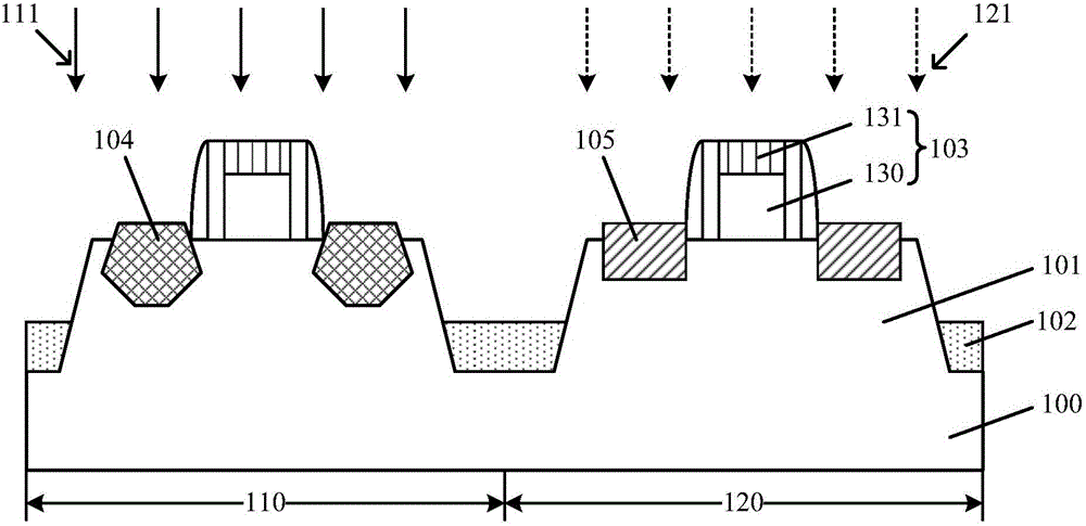
[0032] As described in the background, as the size of semiconductor devices shrinks, the size of the high-K metal-gate transistor is also reduced accordingly, which increases the difficulty of manufacturing the high-K metal-gate transistor, resulting in a decrease in the performance of the high-K metal-gate transistor.

[0033] After research, it is found that since the high-K metal gate transistor is formed by the Gate Last process, however, as the size of semiconductor devices shrinks and the device density increases, in the process of the Gate Last process, the gap between adjacent dummy gate structures The aspect ratio of the trench between them increases, which increases the difficulty of filling the dielectric layer, and the density of the formed dielectric layer is poor, which not only affects the insulation performance of the formed dielectric layer, but also causes the formation of adjacent gates. The parasitic capacitance between pole structures increases, resulting i...


PUM

PropertyMeasurementUnit
Thicknessaaaaaaaaaa
Thicknessaaaaaaaaaa

Abstract

The invention discloses a semiconductor structure forming method. The method comprises steps: a substrate is provided, wherein the substrate comprises a first area and a second area, surfaces of the first area and the second area of the substrate are provided with pseudo gate structures respectively, and the pseudo gate structure comprises a pseudo gate layer and an initial mask layer located on the surface of the pseudo gate layer; a first stress layer is formed in the substrate at two sides of the pseudo gate structure in the first area; a first deep injection process is adopted to dope ions of a first type in the first stress layer and in the partial substrate at the bottom part of the first stress layer; after the first deep injection process, the thickness of the initial mask layer is thinned, and a first mask layer is formed; a second source-drain area is formed in the substrate at two sides of the pseudo gate structure in the second area; and after the first mask layer and the second source-drain area are formed, a dielectric layer is formed on the surface of the substrate, the dielectric layer covers the side wall surface of the pseudo gate structure, and the surface of the dielectric layer is flush with the top surface of the first mask layer. The performance of the formed semiconductor structure is improved.

Description

technical field [0001] The invention relates to the technical field of semiconductor manufacturing, in particular to a method for forming a semiconductor structure. Background technique [0002] With the rapid development of integrated circuit manufacturing technology, the size of semiconductor devices in integrated circuits, especially MOS (Metal Oxide Semiconductor, metal-oxide-semiconductor) devices, is continuously reduced to meet the miniaturization and development of integrated circuits. Integration requirements, and transistor devices are one of the important components of MOS devices. [0003] For transistor devices, as the size of the transistor continues to shrink, the gate dielectric layer formed of silicon oxide or silicon oxynitride material in the prior art cannot meet the performance requirements of the transistor. In particular, transistors formed with silicon oxide or silicon oxynitride as the gate dielectric layer are prone to a series of problems such as ...

Claims


Application Information

Patent Timeline
IPC IPC(8): H01L21/8238H01L27/092
CPCH01L27/0924H01L21/823814H01L21/823821H01L21/823864
Inventor 周飞
Owner SEMICON MFG INT (SHANGHAI) CORP
Why Eureka
Try Eureka