Manufacturing method of micro-electromechanical device, micro-electromechanical device and micro-electromechanical device base structure

A manufacturing method and technology of electrical devices, applied in the direction of manufacturing microstructure devices, microelectronic microstructure devices, microstructure technology, etc., can solve the problems of weak strength of the device layer 12, increase of manufacturing cost, contamination of the device layer, etc., and achieve improved Operability, improve yield, meet the effect of small-size device manufacturing

Inactive Publication Date: 2017-02-08
苏州工业园区纳米产业技术研究院有限公司
View PDF8 Cites 2 Cited by
  • Summary
  • Abstract
  • Description
  • Claims
  • Application Information

AI Technical Summary

Problems solved by technology

However, see figure 1 and figure 2 , when etching the silicon substrate 11, due to the weak strength of the thinner device layer 12, the thin film of the device layer 12 is prone to damage
The damaged device layer 12 will contaminate or even damage the machine, which will increase the manufacturing cost and even make mass production impossible
[0004] In addition, due to the possibility of etching deviation during dry etching of the substrate, in order to compensate for the deviation of dry etching, it is usually necessary to etch the bottom substrate by overetching, so it is easy to etch the bottom substrate. damage device layer 12 during etching

Method used


Image

  • Manufacturing method of micro-electromechanical device, micro-electromechanical device and micro-electromechanical device base structure
  • Manufacturing method of micro-electromechanical device, micro-electromechanical device and micro-electromechanical device base structure
  • Manufacturing method of micro-electromechanical device, micro-electromechanical device and micro-electromechanical device base structure

Examples


Embodiment Construction

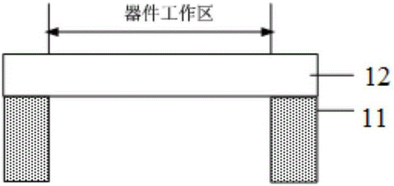
[0033] The specific implementation manners of the present invention will be further described in detail below in conjunction with the accompanying drawings and embodiments. The following examples are used to illustrate the present invention, but are not intended to limit the scope of the present invention. The up, down, left, right, front, back and Figure 6 The illustrated direction of the MEMS device is the reference, and the up and down direction is the height direction of the MEMS device.

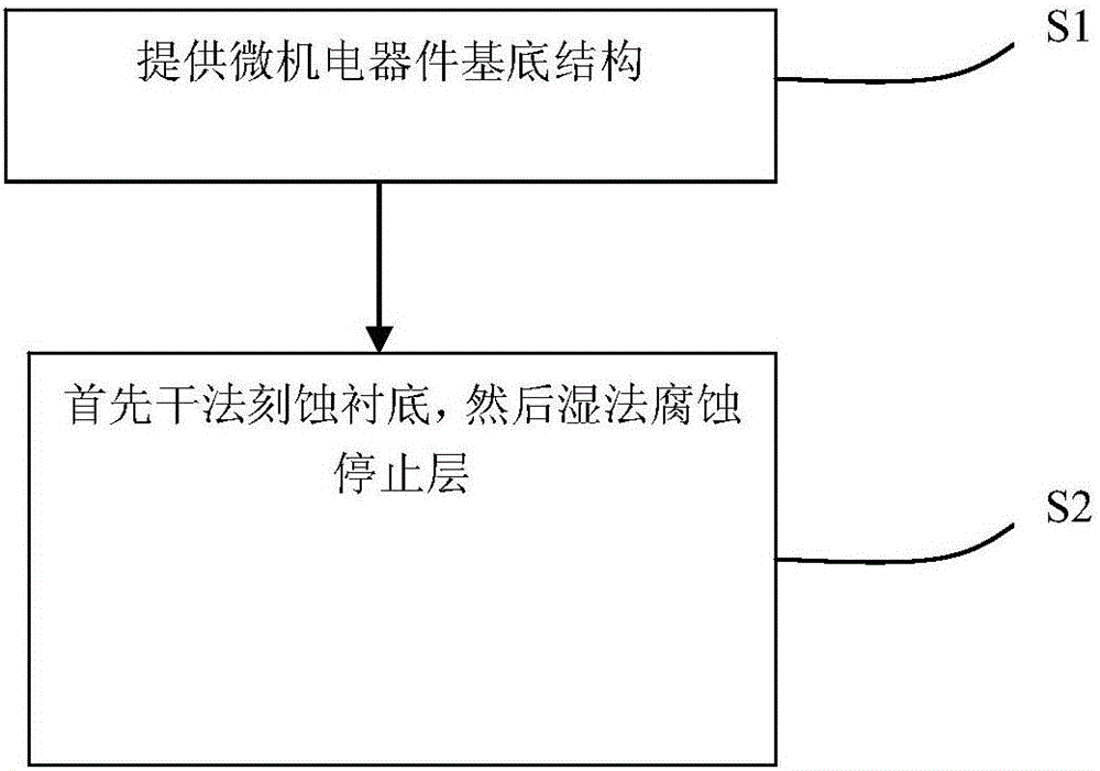
[0034] See image 3 , and combined with Figure 4 to Figure 6 , the manufacturing method of the MEMS device shown in embodiment 1 comprises the following steps:

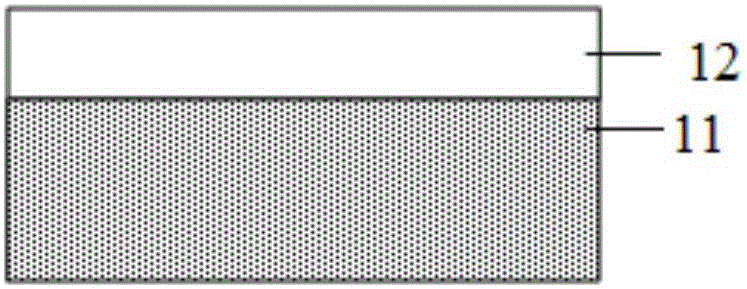
[0035] S1: Provide a microelectromechanical device base structure 20, the microelectromechanical device base structure 20 includes a substrate 21 having a lower surface 211 and an upper surface 212, and at least one stop layer 22 disposed on the upper surface 212 of the substrate 21 , 23 and a device layer 24 disposed on t...


PUM


Abstract

The invention relates to a manufacturing method of a micro-electromechanical device, a micro-electromechanical device and a micro-electromechanical device base structure. The manufacturing method of the micro-electromechanical device comprises the following steps: S1: providing a micro-electromechanical device base structure, wherein the micro-electromechanical device base structure comprises a substrate provided with an upper surface and a lower surface, at least one stop layer arranged on the upper surface of the substrate, and a device layer arranged on the topmost stop layer, wherein the substrate and the stop layer most adjacent to the substrate are made from different materials; and S2: etching the substrate by a dry process, and etching the stop layer(s) by a wet process. In the dry-process substrate etching according to the manufacturing method, the etching firstly stops at the stop layer, and the stop layer is etched by the wet-process etching technique; and thus, in the dry-process etching, the stop layer is utilized to enhance the strength of the device layer so as to avoid the damage of the device layer, thereby enhancing the yield and satisfying the manufacturing of minisize devices.

Description

technical field [0001] The invention relates to a manufacturing method of a microelectromechanical device, a microelectromechanical device and a base structure of the microelectromechanical device. Background technique [0002] Silicon is widely used in IC manufacturing and MEMS manufacturing because of its superior mechanical and electrical properties. In order to meet the manufacturing requirements of various geometric shapes such as pits, holes, teeth, etc., it is mainly obtained by dry etching and wet etching. When etching the back cavity of the device, KOH solution or TMAH can be used as the etching solution. However, the etching rate of this method is slower than that of dry deep silicon etching (DRIE), and at the same time, the sidewall forms a 54.74-degree inclination angle with the silicon wafer surface, resulting in a larger chip area. DRIE uses the Bosch process of etching and sidewall protection alternately to protect the sidewall, which can achieve controllabl...

Claims


Application Information

Patent Timeline
IPC IPC(8): B81C1/00B81B7/02
CPCB81C1/00349B81B7/02B81B2201/02B81B2201/0278
Inventor 宋焱韩冬马清杰
Owner 苏州工业园区纳米产业技术研究院有限公司
Why Eureka
Try Eureka