Ultraviolet emitting material surface photovoltage spectrum testing device and testing method

A surface photovoltage spectrum and emission material technology, which is applied in the field of ultraviolet emission material surface photovoltage spectrum test equipment, can solve the problem that the optical fiber has a large loss in the ultraviolet band, cannot meet the surface photovoltage spectrum test requirements of ultraviolet emission materials, and the ultraviolet emission material cannot generate surface photovoltage. Signal and other problems to achieve the effect of reducing interference

Inactive Publication Date: 2017-02-08
NANJING UNIV OF SCI & TECH
View PDF4 Cites 8 Cited by
  • Summary
  • Abstract
  • Description
  • Claims
  • Application Information

AI Technical Summary

Problems solved by technology

In the existing surface photovoltage spectrum testing device, since the spectral range of the light source is in the visible light range, the loss of the optical fiber to the ultraviolet band is too large, and the transparent conductive glass is made of ordinary ITO glass, which is basically impermeable to ultraviolet light, so that the tested ultraviolet emitting material cannot produce the required The surface photovoltage signal cannot meet the test requirements of the surface photovoltage spectrum of ultraviolet emitting materials. There is an urgent need for testing devices and methods that can directly measure the surface photovoltage spectrum of ultraviolet emitting materials to obtain performance parameters such as minority carrier diffusion length and surface recombination rate of ultraviolet emitting materials.

Method used


Image

  • Ultraviolet emitting material surface photovoltage spectrum testing device and testing method
  • Ultraviolet emitting material surface photovoltage spectrum testing device and testing method
  • Ultraviolet emitting material surface photovoltage spectrum testing device and testing method

Examples


Embodiment

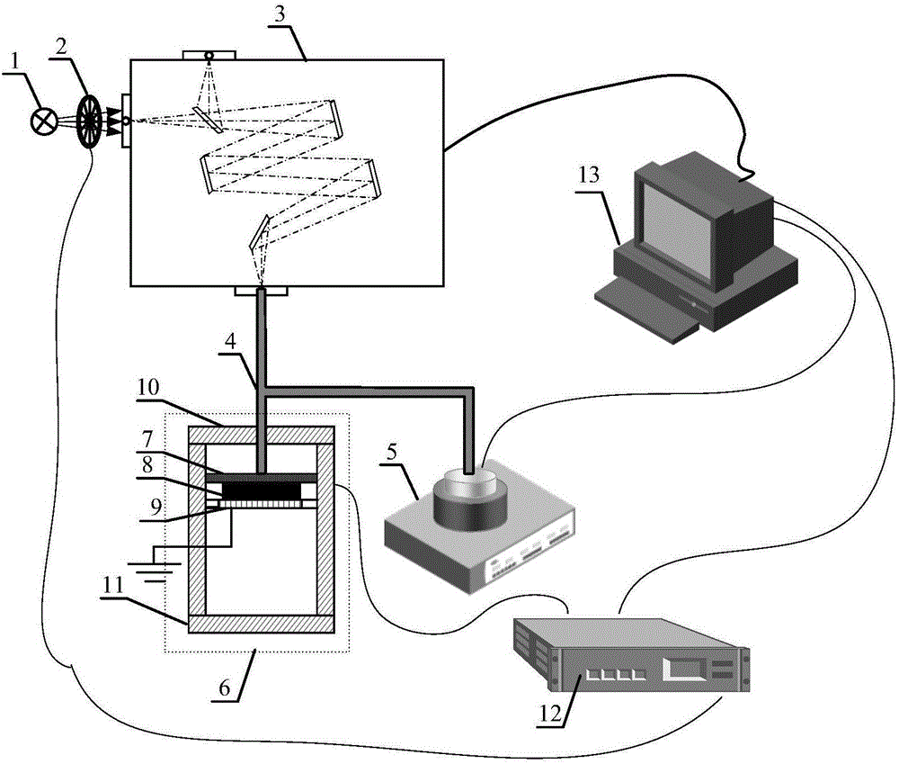
[0042] combine figure 1 , a surface photovoltage spectrum testing device for ultraviolet emitting materials, comprising a deuterium lamp light source 1, a light chopper 2, a grating monochromator 3, an ultraviolet splitting optical fiber 4, an optical power meter 5, a photovoltage cell 6, a lock-in amplifier 12 and computer13.

[0043] A chopper 2 is placed between the deuterium light source 1 and the grating monochromator 3; the incident end of the ultraviolet splitting fiber 4 is connected to the light outlet of the grating monochromator 3, and the output end is connected to the photovoltage cell 6 and the optical power meter 5 respectively; The signal output terminal of the pool 6 is connected with the signal input terminal of the lock-in amplifier 12; the communication port of the optical power meter 5 and the lock-in amplifier 12 is connected with the computer 13 serial port.

[0044] The deuterium light source 1 and the grating monochromator 3 are combined to form a wav...


PUM


Abstract

The invention discloses an ultraviolet emitting material surface photovoltage spectrum testing device, which comprises a deuterium lamp light source, a chopper, a grating monochromator, an ultraviolet light-splitting optical fiber, an optical power meter, a photovoltage pool, a phase-locked amplifier and a computer, and is characterized in that the chopper is placed between the deuterium lamp light source and the grating monochromator; an incoming end of the ultraviolet light-splitting optical fiber is connected with a light outlet of the grating monochromator, a outgoing end of the ultraviolet light-splitting optical fiber is connected with the photovoltage pool and the optical power meter; a signal output end of the photovoltage pool is connected with a signal input end of the phase-locked amplifier; communication ports of the optical power meter and the phase-locked amplifier are connected with serial ports of the computer. According to the invention, the completely closed ultraviolet light-splitting optical fiber is adopted, so that interference imposed on surface photovoltage signals by external stray light can be effectively reduced; conductive glass in the photovoltage pool adopts deep-ultraviolet transparent conductive glass, so that ultraviolet emitting material surface photovoltage signals with high intensity and good stability can be acquired.

Description

technical field [0001] The invention relates to the technical field of semiconductor material testing, in particular to a photovoltage spectrum testing device and a testing method for the surface of an ultraviolet emitting material. Background technique [0002] For semiconductor vacuum photodetection devices, parameters such as minority carrier diffusion length and surface recombination rate of semiconductor cathode emitting materials have a crucial influence on spectral response and electron escape probability. At present, the methods for studying the properties of the surface of semiconductor materials mainly include X-ray photoelectron spectroscopy, ultraviolet photoelectron spectroscopy and surface photovoltage spectroscopy. Compared with the former two, surface photovoltage spectroscopy has the characteristics of non-destructive and non-contact, simple equipment, and high sensitivity, and is very suitable for testing parameters such as minority carrier diffusion length...

Claims


Application Information

Patent Timeline
IPC IPC(8): G01R31/26
CPCG01R31/2648
Inventor 钱芸生刘健冯琤王岩
Owner NANJING UNIV OF SCI & TECH
Why Eureka
Try Eureka