PoP (Package on Package) automatic stacking system and method

A technology of automatic stacking and operation methods, applied in the fields of electrical components, semiconductor/solid-state device manufacturing, circuits, etc., can solve problems such as poor precision, low efficiency, and difficulty in ensuring product quality consistency, and achieve strong platform versatility and reliability The effect of manufacturability and precise control of stack height

Active Publication Date: 2017-02-15
郑州兴航科技有限公司
View PDF4 Cites 8 Cited by
  • Summary
  • Abstract
  • Description
  • Claims
  • Application Information

AI Technical Summary

Problems solved by technology

The method of mold stacking and manual stacking is inefficient in mass production. When there is a need for higher interlayer stacking accuracy (such as accuracy error ≤ 40μm), the accuracy is po...

Method used


Image

  • PoP (Package on Package) automatic stacking system and method
  • PoP (Package on Package) automatic stacking system and method
  • PoP (Package on Package) automatic stacking system and method

Examples


Embodiment 1

[0091] 3D stack assembly of completed assembled planar substrate circuits

[0092] Various components are assembled on the planar substrate circuit (such as Figure 20 and Figure 21 shown), in order to prevent component damage on the planar circuit assembly, stack mounting cannot be performed directly. When mounting interlayer spacers, suction can be applied simultaneously at two or more point positions of board-type components by using dual / multi-head nozzles. Paste epoxy adhesive film or apply quick-curing glue on the bonding position on the interlayer backing plate through the dispensing system, which can be stacked through the interlayer frame (such as Figure 17 , Figure 18 and Figure 19shown). The inter-layers are pre-fixed by epoxy adhesive film or fast-curing glue, which can maintain the assembly accuracy between the layers of the stack before further reinforcement.

Embodiment 2

[0094] Mount easily deformable sheet

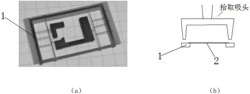
[0095] The main body of the stack is a plastic-encapsulated chip, but a layer of copper foil 2 with a thickness of only 100 μm and a hollow pattern (such as image 3 shown). Because the copper foil 2 is extremely thin, it is easy to curl and deform, causing it to be unrecognizable by normal camera equipment, and it is difficult to pick it up with a single suction head. By attaching the copper foil 2 on the interlayer spacer, you can rely on the reinforcement function of the interlayer spacer and ensure that it can use double suction heads to achieve normal automatic pick-and-place (such as image 3 and Figure 4 shown).

[0096] see Figure 12 , Figure 13 and Figure 14 As shown, the structure of the interlayer cushion frame 1 can adopt the shape of "concave", "back", etc., and the thickness needs to be controlled. If the planned single-layer height is H, and the thickness of the substrate is a, the interlayer bonding material (adh...

Embodiment 3

[0109] Stacking monolithic components is performed in the following steps

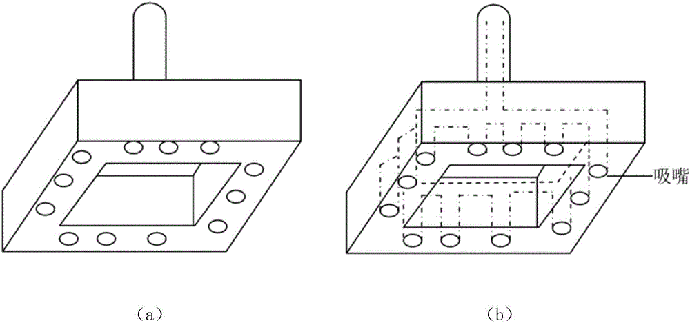
[0110] 1) Use the image recognition software to cooperate with the camera system to identify the positioning points / positioning graphics on the single-chip components (see Figure 6 , Figure 10 , Figure 11 );

[0111] 2) The program manipulates the pick-up head for single-chip components, picks up the first layer of single-chip components and places them on the stacked mold;

[0112] 3) Identify and pick up the epoxy film for interlayer bonding, and place it at the designated bonding position of the first layer of monolithic components;

[0113] 4) Identify and pick up the second layer of monolithic components, through the identification system, confirm the positioning point that the upper and lower layers need to be aligned, then move the second layer of monolithic components to the specified position, and lower the pick-up head to make the second layer The component is pressed on the epoxy film...


PUM

PropertyMeasurementUnit
Thicknessaaaaaaaaaa

Abstract

The invention discloses a PoP (Package on Package) automatic stacking system and method. The PoP automatic stacking system comprises a pick-up suction head, a stacking mold base, an image recognition system and a dispensing system, wherein the pick-up suction head recognizes and positions planar circuits through the image recognition system, and fixes the planar circuits to the stacking mold base in a stacking way; and after being dispersed through the dispensing system, the planar circuits are heated and pressed to perform interlayer mounting. The PoP automatic stacking system and method have relatively high extensibility, and can be widely applied to implementation of high-accuracy three-dimensional automatic laminated assembly of various TSOP (Thin Small Outline Package) packaged single-chip devices and planar circuit assemblies. Mechanization of a full set of stacking actions is realized, so that the laminating efficiency, yield and product quality consistency can be increased and improved through stability and accuracy of mechanical equipment. The PoP automatic stacking system and method have very wide application prospects.

Description

[0001] 【Technical field】 [0002] The invention belongs to the field of assembly technology, and in particular relates to a system and method for performing PoP (Package on Package) automatic three-dimensional stack assembly on planar circuits (such as plastic-encapsulated chips, assembled soldered printed boards, etc.). [0003] 【Background technique】 [0004] As various electronic systems become more and more powerful and complex, the number of internal computers is gradually increasing, resulting in an increase in the size and weight of the electronic system. Therefore, how to reduce the size and weight of the computer is becoming more and more important The attention of designers in the aerospace field. The use of three-dimensional stacked packaging technology can greatly increase the assembly density of circuit components and solve the bottleneck problem of circuit component volume and weight. [0005] Three-dimensional laminated assembly and three-dimensional interconnec...

Claims


Application Information

Patent Timeline
IPC IPC(8): H01L21/67
CPCH01L21/67121
Inventor 张丁
Owner 郑州兴航科技有限公司
Why Eureka
Try Eureka