Formation method of semiconductor structure

A semiconductor and conductive layer technology, applied in semiconductor/solid-state device manufacturing, electrical components, circuits, etc., can solve the problem that the electrical performance of semiconductor structures needs to be improved

Active Publication Date: 2017-02-15
SEMICON MFG INT (SHANGHAI) CORP +1
View PDF4 Cites 4 Cited by
  • Summary
  • Abstract
  • Description
  • Claims
  • Application Information

AI Technical Summary

Problems solved by technology

[0004] However, the electrical properties of semiconductor stru

Method used


Image

  • Formation method of semiconductor structure
  • Formation method of semiconductor structure
  • Formation method of semiconductor structure

Examples


Embodiment Construction

[0032] It can be seen from the background art that the electrical performance of the semiconductor structure formed in the prior art needs to be improved.

[0033] The method for forming a semiconductor structure includes the following steps:

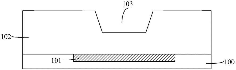
[0034] refer to figure 1 1. Provide a substrate 100, the base metal layer 101 is formed inside the substrate 100, and a dielectric layer 102 is formed on the surface of the substrate 100; a partial thickness of the dielectric layer 102 is etched, and a pre-opening 103 is formed in the dielectric layer 102.

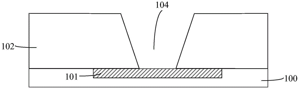
[0035] refer to figure 2 , etch at the pre-opening 103 (refer to figure 1 ) below the dielectric layer 102 to form an opening 104 penetrating through the dielectric layer 102, and the bottom of the opening 104 exposes the surface of the underlying metal layer 101; a conductive layer filling the opening 104 is formed.

[0036] In the above method, the underlying metal layer 101 is severely damaged by etching, which makes the el...


PUM


Abstract

A formation method of a semiconductor structure comprises the steps of providing a substrate in which a bottom-layer metal layer is formed; forming an etching barrier layer covering the surfaces of the substrate and the bottom-layer metal layer; forming a dielectric layer covering the surface of the etching barrier layer; forming an opening penetrating the dielectric layer, and exposing the surface of the etching barrier layer out of the bottom of the opening; adopting a dry etching process of an etching gas containing CF3I to etch a part of thickness of etching barrier layer located at the bottom of the opening, and forming a protection layer on the surface of the side wall of the opening while etching the part of thickness of etching barrier layer; after the protection layer is formed, adopting an isotropy dry etching process to etch and remove the residual thickness of etching barrier layer until the top surface of the bottom-layer metal layer is exposed; forming a conductive layer on the surface of the exposed bottom-layer metal layer, wherein the conductive layer fills the opening. According to the present invention, the etching damage to the bottom-layer metal layer is reduced, and the electrical property of the semiconductor structure is improved.

Description

technical field [0001] The invention relates to the technical field of semiconductor manufacturing, in particular to a method for forming a semiconductor structure. Background technique [0002] With the continuous advancement of VLSI process technology, the feature size of semiconductor devices has been continuously reduced, and the chip area has continued to increase. The delay time of the interconnect structure can be compared with the device gate delay time. People are faced with the problem of how to overcome the significant increase in RC (R refers to resistance, C refers to capacitance) delay due to the rapid increase in connection length. In particular, due to the increasing influence of the capacitance between metal wirings, the performance of the device is greatly reduced, which has become a key restrictive factor for the further development of the semiconductor industry. In order to reduce the RC delay caused by interconnection, various measures have been adopted...

Claims


Application Information

Patent Timeline
IPC IPC(8): H01L21/768H01L21/3065
CPCH01L21/3065H01L21/76804H01L21/76814
Inventor 张海洋周俊卿
Owner SEMICON MFG INT (SHANGHAI) CORP
Why Eureka
Try Eureka