Thin film transistor array substrate, manufacturing method thereof and display panel

A thin film transistor and array substrate technology, applied in the display field, can solve the problems of large off-state current, high manufacturing cost, slow response speed of thin film transistors, etc., and achieve the effects of small leakage current and high switching current ratio

Active Publication Date: 2017-02-15
BOE TECH GRP CO LTD +1
View PDF4 Cites 2 Cited by
  • Summary
  • Abstract
  • Description
  • Claims
  • Application Information

AI Technical Summary

Problems solved by technology

[0005] In view of this, it is necessary to provide a thin film transistor array substrate, its manufacturing method and display panel to solve the problem that in the existing thin film transistors, the mobility of carriers in the active layer is low, resulting in a slow response speed of the thin film transistors. Slow, or the preparation cost is higher, the method is more complicated, the off-state current is larger, etc.

Method used


Image

  • Thin film transistor array substrate, manufacturing method thereof and display panel
  • Thin film transistor array substrate, manufacturing method thereof and display panel
  • Thin film transistor array substrate, manufacturing method thereof and display panel

Examples


Embodiment Construction

[0015] In order to make the technical problems, technical solutions and advantages to be solved by the present invention clearer, the following will describe in detail with reference to the drawings and specific embodiments.

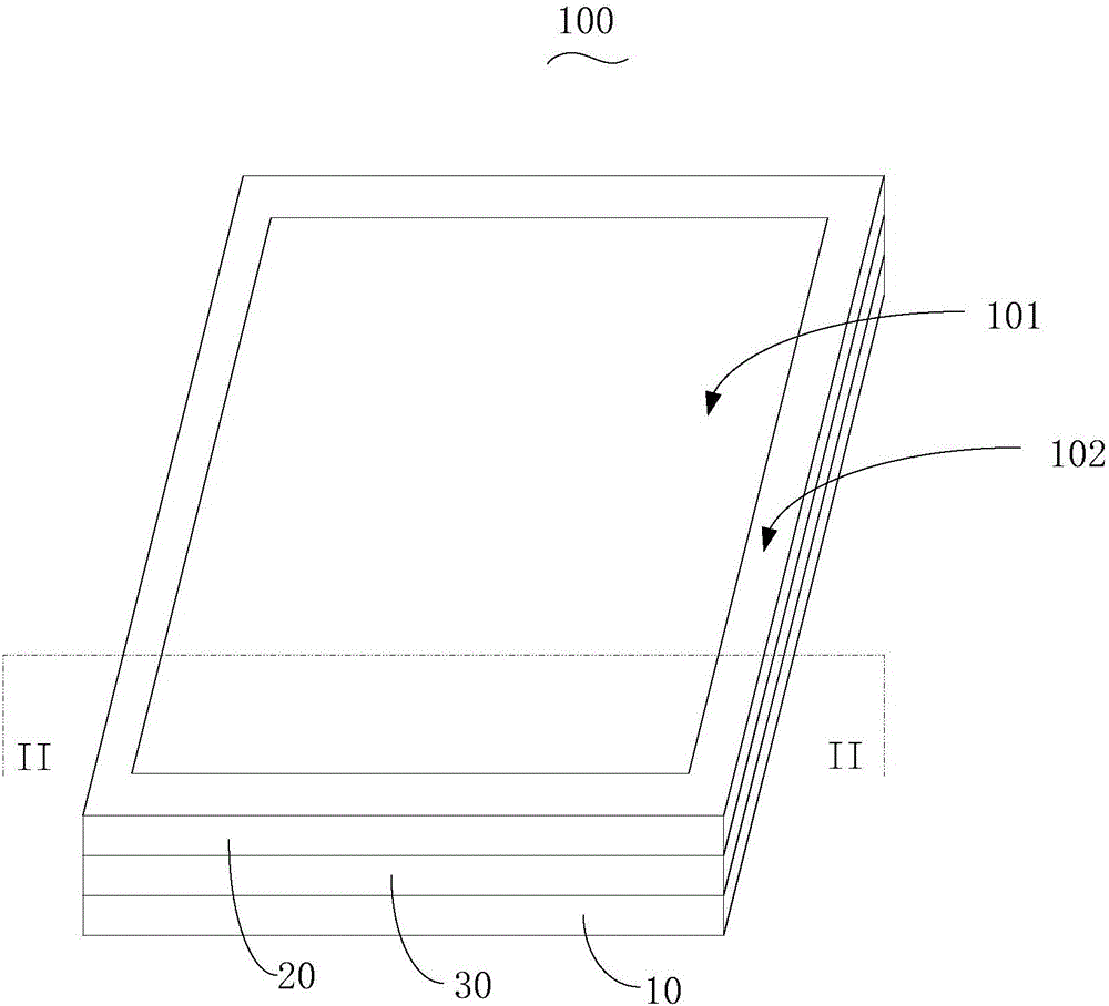
[0016] Such as figure 1 as shown, figure 1 A perspective view of a display device provided by a preferred embodiment of the present invention. The display device 100 includes a first substrate 10 , a second substrate 20 opposite to the first substrate 10 , and a liquid crystal layer 30 between the first substrate 10 and the second substrate 20 . The display device 100 also includes a display area 101 and a peripheral area 102 surrounding the display area 101 , the display area 101 is used to realize the display function of the display device.

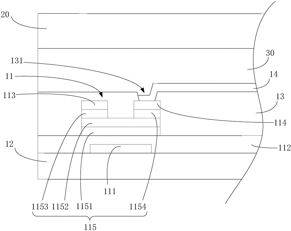
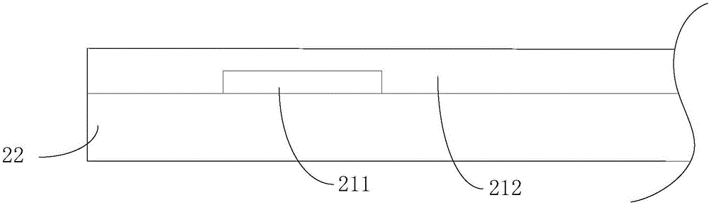
[0017] In this embodiment, the first substrate is a thin film transistor array substrate, and the second substrate is a color filter substrate, but they are not limited thereto. In other embodiments, the first s...


PUM


Abstract

The invention provides a thin film transistor array substrate, a manufacturing method thereof and a display panel. The thin film transistor array substrate comprises thin film transistors, wherein each thin film transistor is internally provided with an active layer composed of a carbon nanotube semiconductor layer and a non-doped amorphous silicon layer, and the non-doped amorphous silicon layer is arranged between the corresponding carbon nanotube semiconductor layer and a source as well as a drain. Therefore, when the thin film transistor is turned on, electricity is mainly conducted by means of the carbon nanotube semiconductor layer in the active layer, and the carbon nanotube semiconductor layer has high electron mobility and forms a high ON-state current; and when the thin film transistor is turned off, a leakage current is mainly released by means of the non-doped amorphous silicon layer in the active layer, and the leakage current is small, thus the thin film transistor has a high switching current ratio.

Description

technical field [0001] The invention relates to the field of display technology, in particular to a thin film transistor array substrate, a manufacturing method thereof and a display panel. Background technique [0002] The demand for various display devices has increased with the rise of the global information society. Therefore, much effort has been devoted to the research and development of various flat display devices, such as liquid crystal displays (LCDs), plasma display panels (PDPs), electroluminescent displays (ELDs), and vacuum fluorescent displays (VFDs). [0003] Thin Film Transistor (TFT) is a key electronic component in modern microelectronics technology, and has been widely used in fields such as flat panel displays. In practical applications, the requirement for thin film transistors is to obtain a larger switching current ratio. Factors Affecting the On-Off Current Ratio The carrier mobility of the semiconductor material in the active layer of the thin-fil...

Claims


Application Information

Patent Timeline
Patent Type & Authority Applications(China)
IPC IPC(8): H01L27/12H01L29/16H01L29/165H01L21/84
CPCH01L27/1229H01L27/127H01L29/1604H01L29/165
Inventor 白金超刘建涛郭会斌
Owner BOE TECH GRP CO LTD
Why Eureka
Try Eureka