Integrated chip of enhanced and depletion type HEMT device and preparation method

An integrated chip, depletion-mode technology, used in semiconductor/solid-state device manufacturing, semiconductor devices, electric solid-state devices, etc., can solve problems such as uneven distribution of device threshold voltages, risk of false turn-on, and large gate leakage current. Achieve the effect of weakening the polarization electric field strength of the barrier layer, weakening the polarization electric field strength, and reducing power consumption

Active Publication Date: 2021-04-06
View PDF6 Cites 1 Cited by
  • Summary
  • Abstract
  • Description
  • Claims
  • Application Information

AI Technical Summary

Problems solved by technology

[0004] However, when the depletion-mode GaN HEMT device is prepared by completely etching the P-type nitride layer in the above method, there is dry etching damage on the surface of the AlGaN layer below the gate region, which will cause a large amount of damage on the surface of the AlGaN layer. Defects, resulting in uneven distribution of device threshold voltage and large gate leakage current
At the same time, the enhanced HEMT device prepared by selectively etching the P-type nitride layer has a low threshold voltage. In actual circuit applications, there is a risk of false turn-on, which affects circuit safety.

Method used


Image

  • Integrated chip of enhanced and depletion type HEMT device and preparation method
  • Integrated chip of enhanced and depletion type HEMT device and preparation method

Examples


Embodiment 1

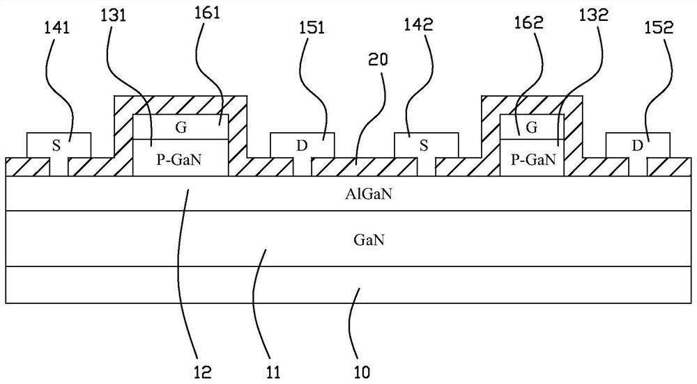
[0031] An integrated chip of enhancement mode and depletion mode HEMT devices, such as figure 1 As shown, it includes a substrate 10, a buffer layer 11, a channel layer, a barrier layer 12, a first P-type nitride gate layer 131, a second P-type nitride gate layer 132, and a first P-type nitride gate layer. The electrode layer 131 and the second P-type nitride gate layer 132 are arranged at intervals; the first P-type nitride gate layer 131 is provided with a first gate metal 161 , and the second P-type nitride gate layer 132 is provided with a second The gate metal 162; the first P-type nitride gate layer 131 and a certain area around it are defined as an enhancement area, and the second P-type nitride gate layer 132 and a certain area around it are defined as a depletion area. The enhancement region usually includes the first P-type nitride gate layer 131, the first gate metal 161, and metal regions such as a certain range around it and a metal-free region; the depletion regi...

Embodiment 2

[0037] The present embodiment provides a method for preparing an integrated chip of an enhanced and depleted HEMT device, for preparing the integrated chip (such as the integrated chip recorded in Example 1), comprising the following steps:

[0038] 1) Prepare a nitride epitaxial structure on the substrate 10. In this embodiment, the nitride epitaxial structure is a P-type nitride HEMT epitaxial structure, including a substrate 10, a GaN buffer layer 11, a channel layer, and an AlGaN barrier layer 12 , P-type nitride gate layer.

[0039] 2) Selectively etch the P-type nitride gate layer to form a first P-type nitride gate layer 131 and a second P-type nitride gate layer 132; wherein, the gate of the first P-type nitride gate layer 131 The electrode line width is greater than the gate line width of the second P-type nitride gate layer 132 . In this embodiment, the gate line width of the first P-type nitride gate layer is 1 μm˜2 μm, and the gate line width of the second P-type ...

Embodiment 3

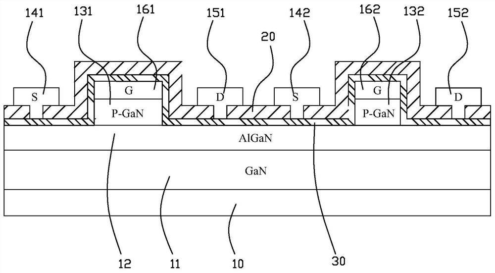
[0046] Such as figure 2 As shown, the difference between this embodiment and Embodiment 1 is that the enhancement region and the depletion region cover the passivation layer 30, and the tensile stress dielectric layer 20 is covered on the passivation layer 30; when PECVD is used to deposit the tensile stress dielectric layer 20 , the plasma bombardment causes damage to the surface of the non-gate region, and a large number of traps are generated on the surface, which reduces the dynamic characteristics of the device.

[0047] In this embodiment, the thickness of the passivation layer 30 is smaller than the thickness of the tensile stress medium layer 20 ; the tensile stress value of the passivation layer 30 is lower than the stress value of the tensile stress medium layer 20 . During specific implementation, the stress value of the passivation layer 30 is -250MPa˜150MPa; the thickness of the passivation layer 30 is less than 20nm. The passivation layer 30 is one or a combina...


PUM

PropertyMeasurementUnit
thicknessaaaaaaaaaa
thicknessaaaaaaaaaa

Abstract

The invention relates to an integrated chip of an enhanced and depletion type HEMT (High Electron Mobility Transistor) device and a preparation method. The correlation between the influence of the stress of a dielectric layer on the threshold voltage of the device and the gate line width of the device is used to regulate and control the stress of a barrier layer below a P-type nitride gate layer and change the polarization electric field intensity of the barrier layer. Finally, monolithic integration of P-type nitride gate enhanced and depletion type HEMT devices is realized. When the depletion type semiconductor device is prepared, the P type nitride layer below the gate metal does not need to be etched, etching damage does not exist on the contact interface of the gate metal and the semiconductor, gate electric leakage of the device can be effectively reduced, the switching current ratio of the device is increased, and power consumption is reduced. Compared with a conventional P-type nitride gate enhanced HEMT, the enhanced semiconductor device prepared by the invention has the advantages that the polarization electric field intensity of the barrier layer below the P-type nitride gate layer is weakened, the polarization charge surface density of a heterojunction interface is reduced, and the threshold voltage of the enhanced semiconductor device is further improved.

Description

technical field [0001] The invention relates to the technical field of semiconductors, and more specifically relates to an integrated chip of an enhanced and depleted HEMT device, and a method for preparing the integrated chip of an enhanced and depleted HEMT device. Background technique [0002] Due to its superior characteristics, silicon-based GaN HEMTs have broad development prospects in the field of power switches. Among them, commercial power GaN HEMTs are mainly P-type nitride gate enhancement HEMT devices. However, due to the low threshold voltage and small gate swing of P-type nitride gate-enhanced HEMT devices, in order to give full play to the advantages of GaN materials, it is necessary to monolithically integrate the gate drive circuit with the power GaN HEMT. [0003] In the prior art, based on the p-GaN / AlGaN / GaN epitaxial structure, a common method for achieving monolithic integration of enhancement-mode and depletion-mode semiconductor devices is: using a dr...

Claims


Application Information

Patent Timeline
Patent Type & Authority Applications(China)
IPC IPC(8): H01L27/085H01L21/8252H01L29/778H01L29/20
CPCH01L27/085H01L21/8252H01L29/778H01L29/2003Y02B70/10
Inventor 刘成田野何俊蕾赵杰郭德霄叶念慈
Why Eureka
Try Eureka