Enhanced and depletion type HEMT integrated device and preparation method

An integrated device, depletion-mode technology, applied in the field of the preparation of enhancement-mode and depletion-mode HEMT integrated devices, can solve the problems of uneven distribution of device threshold voltage, risk of false turn-on, large gate leakage current, etc. The effect of reducing the strength of the electric field, reducing the surface density of the polarization charge, and reducing the power consumption

Active Publication Date: 2021-04-06
HUNAN SANAN SEMICON CO LTD
View PDF9 Cites 1 Cited by
  • Summary
  • Abstract
  • Description
  • Claims
  • Application Information

AI Technical Summary

Problems solved by technology

[0004] However, when the depletion-mode GaN HEMT device is prepared by completely etching the P-type nitride layer in the above method, there is dry etching damage on the surface of the AlGaN layer below the gate region, which will cause a large amount of damage on the surface of the AlGaN layer. Defects, resulting in uneven distribution of device threshold voltage and large gate leakage current
At the same time, the enhanced HEMT device prepared by selectively etching the P-type nitride layer has a low threshold voltage. In actual circuit applications, there is a risk of false turn-on, which affects circuit safety.

Method used


Image

  • Enhanced and depletion type HEMT integrated device and preparation method
  • Enhanced and depletion type HEMT integrated device and preparation method

Examples


Embodiment 1

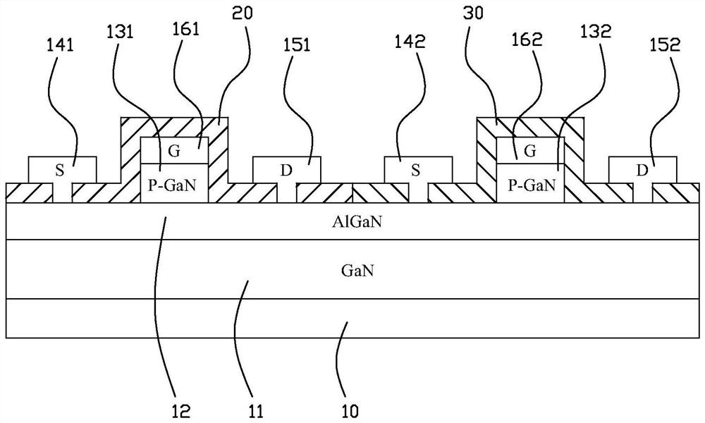
[0056] An integrated enhancement mode and depletion mode HEMT device, such as figure 1 As shown, it includes a substrate 10, a buffer layer 11, a channel layer, a barrier layer 12, a first P-type nitride gate layer 131, a second P-type nitride gate layer 132, and a first P-type nitride gate layer. The electrode layer 131 and the second P-type nitride gate layer 132 are arranged at intervals; the first P-type nitride gate layer 131 is provided with a first gate metal 161 , and the second P-type nitride gate layer 132 is provided with a second The gate metal 162; the first P-type nitride gate layer 131 and a certain area around it are defined as an enhancement area, and the second P-type nitride gate layer 132 and a certain area around it are defined as a depletion area. The enhancement region usually includes the first P-type nitride gate layer 131, the first gate metal 161, and metal regions such as a certain range around it and a metal-free region; the depletion region usuall...

Embodiment 2

[0061] This embodiment provides a method for preparing an enhanced and depleted HEMT integrated device, which is used to prepare the monolithic integrated circuit (such as the monolithic integrated circuit described in Embodiment 1), to first prepare the enhanced semiconductor device, A preparation method for preparing a depletion-type semiconductor device is taken as an example, including the following steps:

[0062] 1) Prepare a nitride epitaxial structure on the substrate 10. In this embodiment, the nitride epitaxial structure is a P-type nitride HEMT epitaxial structure, including a substrate 10, a GaN buffer layer 11, a channel layer, and an AlGaN barrier layer 12 , P-type nitride gate layer; wherein, the substrate includes one of silicon, gallium nitride, silicon carbide, sapphire and other materials.

[0063] 2) Selectively etch the P-type nitride layer to form the first P-type nitride gate layer 131 and the second P-type nitride gate layer 132; in this embodiment, the...

Embodiment 3

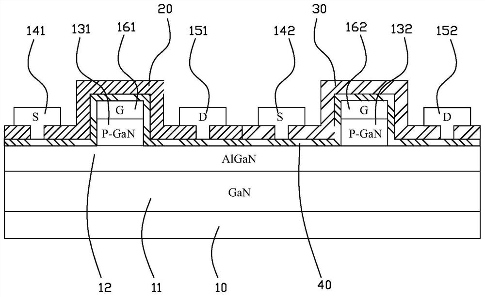
[0070] The difference between this embodiment and Embodiment 2 is that in this embodiment, a depletion-type semiconductor device is prepared first, and then an enhancement-type semiconductor device is prepared. Correspondingly, step 4) and step 5) of this embodiment are as follows:

[0071] 4) Depositing a tensile stress dielectric layer 30 on the surface (entire surface) of the nitride epitaxial structure, the tensile stress dielectric layer 30 covers the enhancement region and the depletion region. During specific implementation, methods such as PECVD and LPCVD can be used to deposit the tensile stress medium layer 30 . After spin-coating photoresist, exposure, and development, the depletion area is covered by photoresist, and the enhancement area is exposed. The tensile stress dielectric layer 30 covering the enhancement area is selectively removed by dry etching (such as ICP, RIE, ECR) or wet etching process. Wherein, the stress medium of the tensile stress medium layer 3...


PUM

PropertyMeasurementUnit
thicknessaaaaaaaaaa
thicknessaaaaaaaaaa

Abstract

The invention relates to an enhanced and depletion type HEMT (high electron mobility transistor) integrated device and a preparation method. Media with different stresses are deposited on a P-type nitride gate layer, the stress of a barrier layer below the P-type nitride gate layer is regulated and controlled, the polarization electric field intensity of the barrier layer is changed, and finally, monolithic integration of P-type nitride gate enhanced and depletion type HEMT devices is realized. When the depletion type semiconductor device is prepared, the P type nitride layer below the gate metal does not need to be etched, etching damage does not exist on the contact interface of the gate metal and the semiconductor, gate electric leakage of the device can be effectively reduced, the switching current ratio of the device is increased, and power consumption is reduced. Compared with a conventional P-type nitride gate enhanced HEMT, the enhanced semiconductor device prepared by the invention has the advantages that the polarization electric field intensity of the barrier layer below the P-type nitride gate layer is weakened, the polarization charge surface density of a heterojunction interface is reduced, and the threshold voltage of the enhanced semiconductor device is further improved.

Description

technical field [0001] The invention relates to the technical field of semiconductors, in particular to an enhanced and depleted HEMT integrated device and a preparation method for the enhanced and depleted HEMT integrated device. Background technique [0002] Due to the superior characteristics of gallium nitride materials, silicon-based GaN HEMTs have broad development prospects in the field of power switches. Among them, commercial power GaN HEMTs are mainly P-type nitride gate enhancement HEMT devices. However, due to the low threshold voltage and small gate swing of P-type nitride gate-enhanced HEMT devices, in order to give full play to the advantages of GaN materials, it is necessary to monolithically integrate the gate drive circuit with the power GaN HEMT. [0003] In the prior art, based on the p-GaN / AlGaN / GaN epitaxial structure, a common method to achieve monolithic integration of enhancement-mode and depletion-mode devices is: use dry etching process to selectiv...

Claims


Application Information

Patent Timeline
Patent Type & Authority Applications(China)
IPC IPC(8): H01L27/085H01L21/8252H01L29/778H01L29/20
CPCH01L27/085H01L21/8252H01L29/778H01L29/2003Y02B70/10
Inventor 蔡文必田野刘成何俊蕾赵杰郭德霄叶念慈
Owner HUNAN SANAN SEMICON CO LTD
Why Eureka
Try Eureka