Fabricating method of flip LED chip provided with DBR (distributed Bragg reflector) formed by using PECVD (plasma enhanced chemical vapor deposition)

An LED chip and manufacturing method technology, applied in electrical components, circuits, semiconductor devices, etc., can solve the problems of complex process technology, difficult material corrosion, long time consumption, etc., and achieve high optical reflectivity, process time saving, and simple production. Effect

Inactive Publication Date: 2017-02-15
JIANGSU XINGUANGLIAN SEMICON
View PDF8 Cites 3 Cited by
  • Summary
  • Abstract
  • Description
  • Claims
  • Application Information

AI Technical Summary

Problems solved by technology

[0003] At present, DBR is usually evaporated SiO by electron beam evaporation table 2 and TiO 2 , arranged periodically according to the ABAB method to enhance the reflectivity of the substrate, but the process takes about 5 hours, which is a long time; and TiO 2 The material is difficult to corrode, and ICP (inductively couple dplasma) dry etching is required, and the process of ICP dry etching takes about 2-3 hours. Therefore, the existing technology for preparing DBR is complex and costly. time consuming

Method used


Image

  • Fabricating method of flip LED chip provided with DBR (distributed Bragg reflector) formed by using PECVD (plasma enhanced chemical vapor deposition)
  • Fabricating method of flip LED chip provided with DBR (distributed Bragg reflector) formed by using PECVD (plasma enhanced chemical vapor deposition)
  • Fabricating method of flip LED chip provided with DBR (distributed Bragg reflector) formed by using PECVD (plasma enhanced chemical vapor deposition)

Examples


Embodiment Construction

[0032] The present invention will be further described below in conjunction with specific drawings and embodiments.

[0033] A fabrication method of a PECVD-deposited DBR flip-chip LED chip in the embodiment, wherein each layer of Si in the DBR layer 3 3 N 4 The thickness of the layer is 52~64nm, each layer of SiO 2 The thickness of the layer is 72~89nm, and the Si 3 N 4 layer and SiO 2 The refractive index of layer is respectively 2.02 and 1.46, is characterized in that: comprises the following steps:

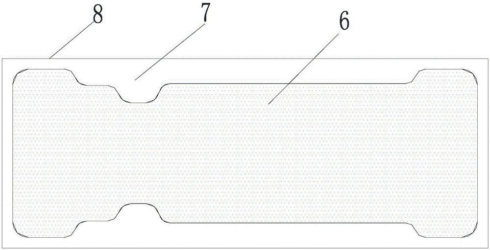
[0034] Such as figure 1 Shown, step 1. Provide a sapphire substrate 8, grow N-type GaN layer 7, quantum well and P-type GaN layer 6 successively on described sapphire substrate 8, complete the epitaxial structure of LED chip;

[0035] Step 2. Etching the P-type GaN layer 6 and the quantum wells in a part of the region through the shielding of the photolithography mask to expose part of the N-type GaN layer 7;

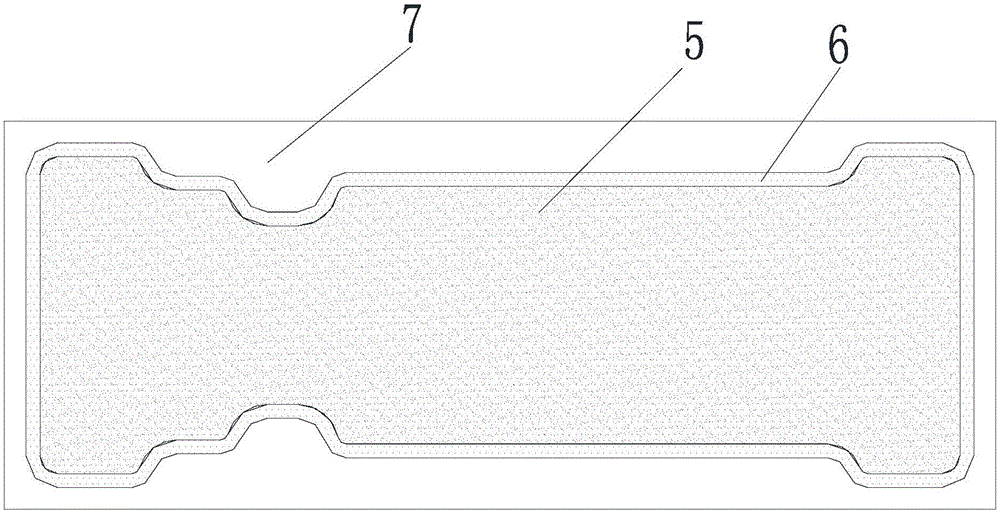
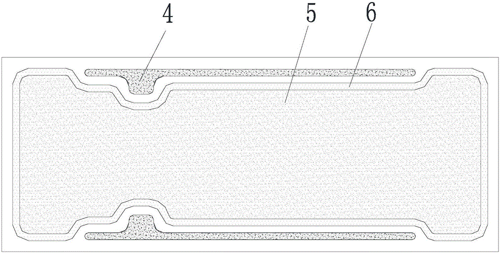
[0036] Such as figure 2 As shown, step 3. Form N-type ext...


PUM

PropertyMeasurementUnit
thicknessaaaaaaaaaa
thicknessaaaaaaaaaa
thicknessaaaaaaaaaa

Abstract

The invention provides a fabricating method of a flip LED chip provided with a DBR (distributed Bragg reflector) formed by using PECVD (plasma enhanced chemical vapor deposition). The method includes the following steps that: an N-type GaN layer, a quantum well and a P-type GaN layer are grown on a sapphire substrate sequentially; a part of the N-type GaN layer is exposed by etching; an N-type extension strip is formed on the exposed N-type GaN layer; a conductive metal layer is fabricated on the surface of the P-type GaN layer; a DBR layer is formed through using the PECVD, wherein the DBR layer is a dielectric film composed of alternately-deposited Si3N4 layers and SiO2 layers; an N electrode window and a P electrode window are respectively formed on the N-type extension strip and the conductive metal layer through BOE wet etching; metal layers are deposited in the electrode windows respectively, so that a negative pad electrode and a positive pad electrode can be formed respectively; the chip is polished, thinned and cut, so that the fabrication of the chip is completed. According to the method of the invention, the PECVD is adopted to alternately deposited the Si3N4 layers and the SiO2 layers, and the alternately-deposited Si3N4 layers and SiO2 layers are adopted as the DBR layer; and the DBR layer is etched through adopting the BOE wet etching. The DBR layer formed by using the method has the advantages of excellent insulation performance, high optical reflectivity, simplicity in fabrication, low cost and short consumed time. With the method adopted, problems in existing flip-chip LED chip technologies can be solved.

Description

technical field [0001] The invention relates to a manufacturing method of a flip-chip LED chip, in particular to a manufacturing method of a flip-chip LED chip with DBR deposited by PECVD (Plasma Enhanced Chemical Vapor Deposition), belonging to the technical field of LED chip manufacturing. Background technique [0002] Now the competition in the LED market is extremely fierce, and the performance requirements for LED chips are constantly improving. At present, DBR is used as the insulating layer and reflective layer for LED flip chips at home and abroad. The entire layer of DBR on the LED chip increases the reflective area without affecting other performance of the chip. At the same time, the brightness is obviously improved; DBR (distributed Bragg reflection), also known as distributed Bragg reflector, is a periodic structure composed of two materials with different refractive indices arranged alternately in the form of ABABA. The optical thickness of each layer of materia...

Claims


Application Information

Patent Timeline
Patent Type & Authority Applications(China)
IPC IPC(8): H01L33/00H01L33/48
CPCH01L33/005H01L33/48
Inventor 闫晓密黄慧诗华斌张秀敏周锋宋凯郑宝玉王顺荣
Owner JIANGSU XINGUANGLIAN SEMICON
Why Eureka
Try Eureka