
Patsnap Eureka
For R&D, Patsnap Eureka makes reading and utilizing patents & technical documents easy.
Patsnap Eureka AIR
Designed for self-driven R&D workflows. Generate viable solutions, solve complex R&D challenges, empower your innovation with AI.

Patsnap Eureka Materials
Designed for material experts only. Revolutionize your material R&D, from search, analyze, to developing new materials.

TechResearch
Generate reliable direction feasibility study reports for your R&D in just a few steps.

TechSeek
Discover and master advanced knowledge NOW. Basics, ideas, possibilities, all at once.

TechMind
As an expert in R&D Theories, TechMind can generates customized viable solutions instantly.

TechRisk
Analyze your overall solution with one click, know your potential R&D risks in advance.

TechMonitor
Get weekly tech updates, stay abreast of the latest tech innovations and key insights.
Photovoltaic cells based on vias through silicon
A technology of photovoltaic cells and through-silicon vias, applied in photovoltaic power generation, photovoltaic modules, circuits, etc., can solve the problems of low and insufficient silicon solar cells
- Summary
- Abstract
- Description
- Claims
- Application Information
AI Technical Summary
Problems solved by technology
Method used
Image

Examples
example 1
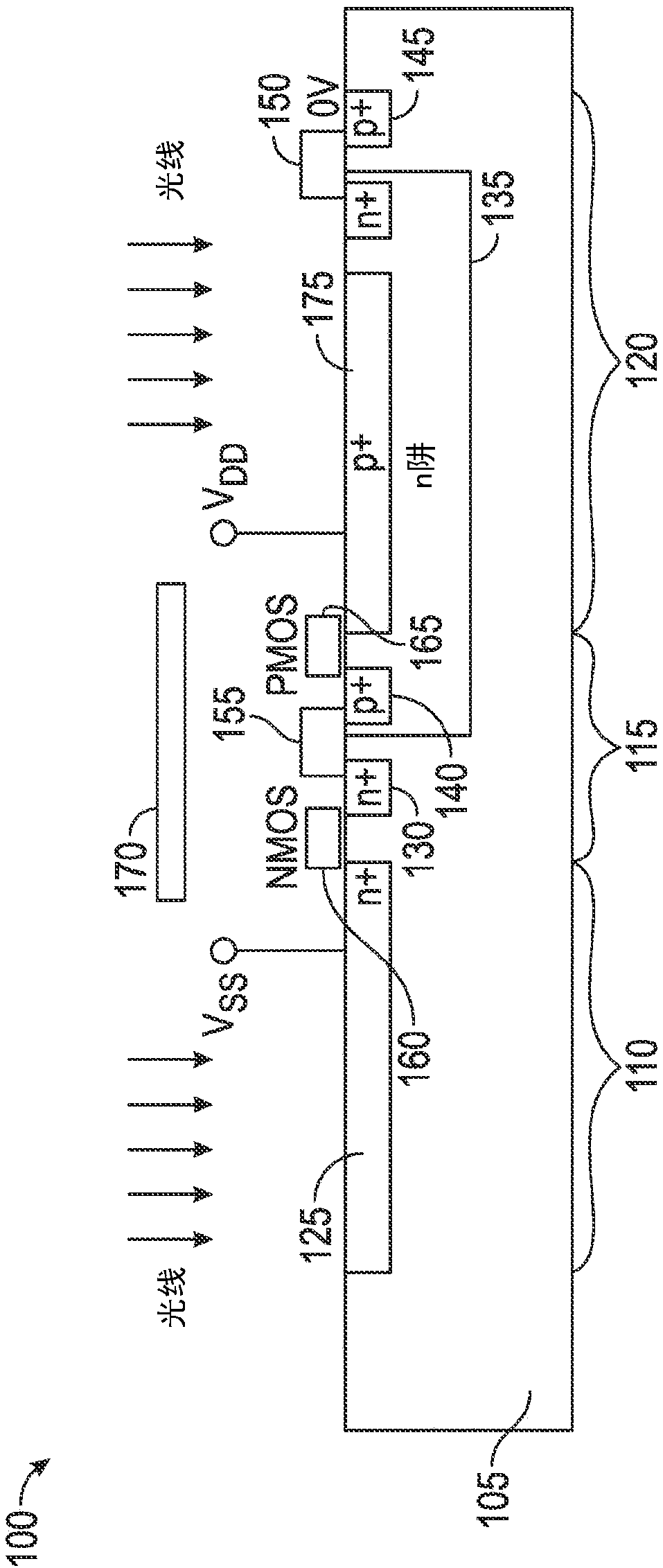
[0038] Example 1 includes an apparatus comprising: a first photovoltaic cell; a first through-silicon via (TSV) included in the first photovoltaic cell and passing through a doped silicon liner At least a portion of the bottom, the first TSV includes (a)(i) a first sidewall that is doped opposite to the doped silicon substrate, and (a)(ii) ) a first contact substantially filling the first TSV; and a second TSV included in the first photovoltaic cell and passing through the doped silicon liner At least another portion of the bottom, the second TSV includes (b)(i) a second sidewall, the second sidewall includes the doped silicon substrate, and (b)(ii) a second contact , the second contact portion substantially fills the second TSV; wherein both the first contact portion and the second contact portion include a substantially transparent conductive material.
[0039] In Example 2, the subject matter of Example 1 can optionally include wherein the first bottom surface of the first...
example 17
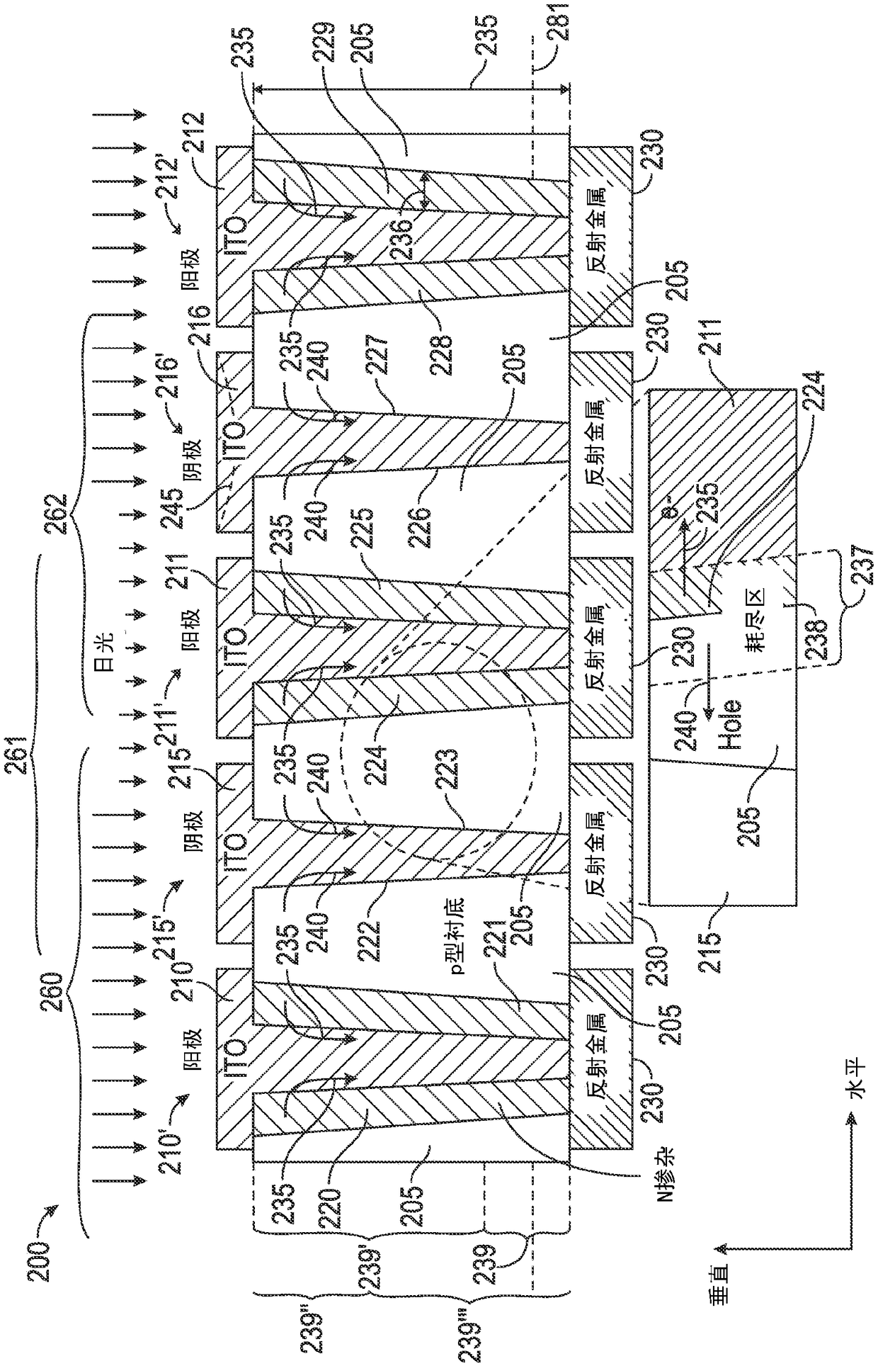
[0054] Example 17 includes an apparatus comprising: a first via included in a first photovoltaic cell and extending from a top surface of a doped substrate to a bottom surface of the doped substrate , the first via hole includes (a)(i) a first sidewall doped opposite to the doped substrate, and (a)(ii) a first contact portion, the first contact substantially filling the first via; and a second via included in the first photovoltaic cell and extending from the top surface to the bottom surface, the second via hole includes (b) (i) a second sidewall, the second sidewall includes the doped substrate, and (b) (ii) a second contact portion, the first The second contact portion substantially fills the second via hole; wherein both the first contact portion and the second contact portion include a transparent conductive material. Again, not all embodiments require TSVs, and some embodiments may use vias (eg, vias extending through non-silicon substrates) or other holes instead of or...
example 21
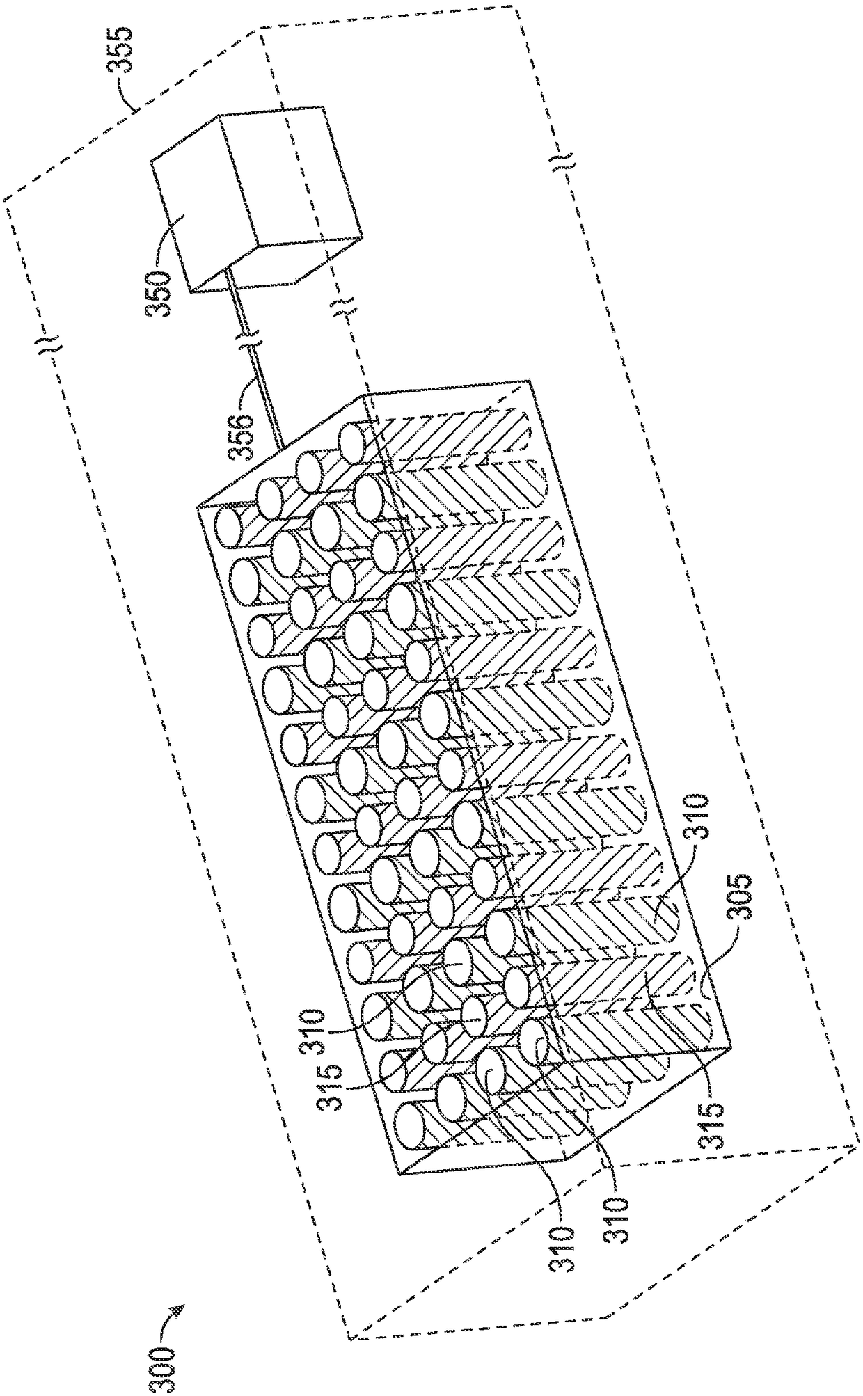
[0058] Example 21 includes a method comprising: forming a reflective metal in direct contact with a bottom surface of a doped substrate; patterning the reflective metal into portions that do not contact each other; forming a first via and a second via holes, the first via hole and the second via hole are included in the first photovoltaic cell, the first via hole and the second via hole each extending from the top surface of the doped substrate to doping the bottom surface of the doped substrate; doping the first sidewall of the first via hole in a manner opposite to that of the doped substrate; and forming a a via and the second via coupled to the first and second contacts of the reflective metal; wherein the first and second contacts each comprise a substantially transparent conductive Material.
[0059] In Example 22, the subject matter of Example 21 can optionally include wherein the first sidewall comprises a PN junction extending from the top of the doped substrate to t...
PUM
 Abstract
Description
Claims
Application Information
 - R&D Engineer
- R&D Manager
- IP Professional
- Industry Leading Data Capabilities
- Powerful AI technology
- Patent DNA Extraction
Browse by: Latest US Patents, China's latest patents, Technical Efficacy Thesaurus, Application Domain, Technology Topic, Popular Technical Reports.
© 2024 PatSnap. All rights reserved.Legal|Privacy policy|Modern Slavery Act Transparency Statement|Sitemap|About US| Contact US: help@patsnap.com