Heterojunction type photoelectric detector and manufacturing method thereof

A photodetector and heterojunction technology, applied in circuits, electrical components, semiconductor devices, etc., can solve problems such as limiting the application of photodetectors, slow response speed, etc., and achieve good ability to receive detected light and high responsivity and gain, the effect of high conductivity

Inactive Publication Date: 2017-03-22
罗雷
View PDF6 Cites 6 Cited by
  • Summary
  • Abstract
  • Description
  • Claims
  • Application Information

AI Technical Summary

Problems solved by technology

The slow response speed will severely limit the application of photodetectors in optoelectronic device integrated circuits

Method used


Image

  • Heterojunction type photoelectric detector and manufacturing method thereof
  • Heterojunction type photoelectric detector and manufacturing method thereof

Examples


Embodiment 1

[0029] In this embodiment, the P-type samarium-doped gallium nitride nanowire and the N-type graphene heterojunction photodetector have the following structure:

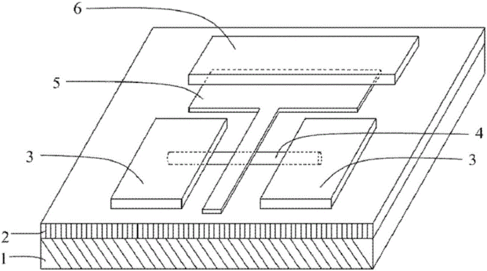
[0030] see figure 1 , on the surface of the silicon substrate 1 covered with the silicon dioxide layer 2, tiled samarium-doped gallium nitride nanowires 4 are dispersed, and 100 nm A thick gold electrode 3 is used as an output pole, and the gold electrode 3 is in ohmic contact with the samarium-doped gallium nitride nanowire 4; graphene is overlapped on the samarium-doped gallium nitride nanowire 4 5. The graphene 5 is located between two gold electrodes 3 and is isolated from the gold electrodes 3; the graphene 5 is provided with a 100 nanometer thick gold electrode 6 as another output pole, and the gold electrode 6 is connected to the gold electrode 3. The graphene 5 is in ohmic contact and is isolated from the samarium-doped gallium nitride nanowire 4 and the gold electrode 3;

[0031] Wherein the samarium-doped...

Embodiment 2

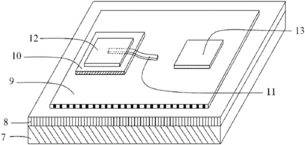
[0035] Such as figure 2 As shown, the P-type samarium-doped gallium nitride nanowire and the N-type graphene heterojunction photodetector in this embodiment have the following structure:

[0036] Graphene 9 is tiled on the surface of the silicon substrate 7 covered with a silicon dioxide layer 8, and a 30 nanometer thick insulating layer 10 is arranged on the graphene 9, and samarium-doped nitrogen is dispersed on the surface of the insulating layer 10 Gallium nitride nanowire 11 and a part of the samarium-doped gallium nitride nanowire 11 is in contact with graphene 9; a 100 nanometer thick gold electrode 12 is arranged on the insulating layer 10, and the gold electrode 12 is connected with samarium-doped nitrogen GaN nanowires 11 are in ohmic contact; 100 nanometer thick gold electrodes 13 are arranged on the graphene 9, and the gold electrodes 13 are isolated from insulating layer 10, gold electrodes 12 and samarium-doped gallium nitride nanowires 11;

[0037] The samariu...


PUM


Abstract

The invention discloses a heterojunction type photoelectric detector and a manufacturing method thereof. The heterojunction type photoelectric detector is composed of p-type samarium-doped gallium nitride nano lines and n-type graphene. The heterojunction type photoelectric detector is advantaged in that the heterojunction type photoelectric detector is quite sensitive to visible light, responsivity and gain are relatively high, a response speed is relatively fast, and excellent bases are provided for application and integration of nano materials in photoelectric devices.

Description

technical field [0001] The invention relates to a heterojunction photodetector of samarium-doped gallium nitride nanowire and N-type graphene and a preparation method thereof. Background technique [0002] Photodetector refers to a physical phenomenon in which the conductivity of the irradiated material is changed by radiation. Photodetectors are widely used in various fields of military and national economy. In the visible or near-infrared band, it is mainly used for ray measurement and detection, industrial automatic control, photometry, etc.; in the infrared band, it is mainly used for missile guidance, infrared thermal imaging, infrared remote sensing, etc. [0003] Photodetectors convert light signals into electrical signals. Depending on the way the device responds to radiation or the mechanism of the device's work, photodetectors can be divided into two categories: one is photon detectors; the other is thermal detectors. According to the device structure, it can be...

Claims


Application Information

Patent Timeline
Patent Type & Authority Applications(China)
IPC IPC(8): H01L31/028H01L31/0304H01L31/109H01L31/18
CPCH01L31/028H01L31/03044H01L31/109H01L31/18Y02P70/50
Inventor 罗雷
Owner 罗雷
Why Eureka
Try Eureka