
Method for improving metallurgical-method polycrystalline silicon growth interface

A technology of polysilicon growth and metallurgy, which is applied in the direction of polysilicon material growth, crystal growth, single crystal growth, etc., can solve the problems of polysilicon performance index instability, differences in propulsion methods, and many defects in the crystal, so as to improve the quality of silicon ingots , good compatibility, process and environment-friendly effect

Inactive Publication Date: 2017-04-19
XINYU UNIV
View PDF4 Cites 3 Cited by
  • Summary
  • Abstract
  • Description
  • Claims
  • Application Information

AI Technical Summary

Problems solved by technology

However, the current conventional metallurgical method to prepare polysilicon materials has uneven distribution of impurities and many intragranular defects, which lead to unstable performance indicators of polysilicon.
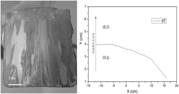
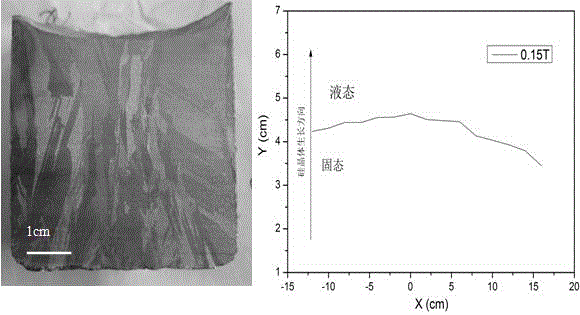
The reason is that during the crystallization and solidification of crystalline silicon, there are large differences in the solid-liquid interface morphology and propulsion mode along the growth direction, which affects the solidification structure characteristics and properties of metallurgical polysilicon.

Method used


Image

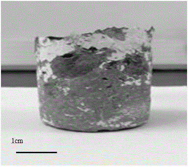
  • Method for improving metallurgical-method polycrystalline silicon growth interface
  • Method for improving metallurgical-method polycrystalline silicon growth interface
  • Method for improving metallurgical-method polycrystalline silicon growth interface

Examples


Embodiment 1

[0017] (1) Preparation stage: put 350g of metallurgical polysilicon material into a high-purity quartz crucible, then put it into a directional solidification furnace, and vacuumize at the same time until the vacuum degree in the furnace is less than 10Pa.

[0018] (2) Heating and melting stage: Start the heating device to raise the furnace temperature to 1450°C to melt the silicon material.

[0019] (3) External field control and crystal growth stage: turn on the static magnetic field generator to apply an axial magnetic field to the molten silicon material for external field control treatment, the magnetic field strength is 0.15T, and the processing time is 15 minutes. Then set the cooling rate of the furnace body to 5°C / min, and the moving part of the furnace body (crucible, graphite holder, graphite separator, base, etc.) to move down at a rate of 10 mm / h, so that the silicon melt slowly detaches from the heater and begins to grow. When the temperature drops to 1100°C, tur...

Embodiment 2

[0022] (1) Preparation stage: put 350g of metallurgical polysilicon material into a high-purity quartz crucible, then put it into a directional solidification furnace, and vacuumize at the same time until the vacuum degree in the furnace is less than 10Pa.

[0023] (2) Heating and melting stage: Start the heating device to raise the furnace temperature to 1450°C to melt the silicon material.

[0024] (3) External field control and crystal growth stage: Turn on the static magnetic field generator to apply an axial magnetic field to the molten silicon material for external field control treatment, the magnetic field strength is 0.2 T, and the processing time is 15 min. Then set the cooling rate of the furnace body to 5°C / min, and the moving part of the furnace body (crucible, graphite holder, graphite separator, base, etc.) to move down at a rate of 10 mm / h, so that the silicon melt slowly detaches from the heater and begins to grow. When the temperature drops to 1100°C, turn of...


PUM

PropertyMeasurementUnit
Diameteraaaaaaaaaa

Abstract

The invention relates to a method for improving a metallurgical-method polycrystalline silicon growth interface. The method comprises the steps: (1) loading polycrystalline-silicon silicon materials to a high-purity quartz crucible, placing the high-purity quartz crucible into a directional solidification furnace, and carrying out vacuumizing until the internal degree of vacuum of the furnace is lower than 10Pa; (2) heating the temperature of the furnace to 1,450 DEG C to 1,550 DEG C so as to melt the silicon materials; (3) carrying out external-field treatment on the silicon materials for 10 to 30 minutes at the magnetic intensity of 0.15T to 0.5T, then, cooling the furnace body at the rate of 5 DEG C / min to 10 DEG C / min, downwards shifting a moving part of the furnace body at the rate of 5mm / h to 10mm / h, enabling silicon melt to be divorced from a heater and start to grow crystals, and closing a magnetic field when the temperature is 1,100 DEG C to 1,200 DEG C; and (4) after crystal growth, enabling the moving part of the furnace body to rise to an initial position in a furnace chamber at the rate of 2mm / s to 4mm / s, then, heating the temperature to 1,250 DEG C to 1,350 DEG C, carrying out heat preservation for 2 to 5 hours, and then, carrying out cooling at the cooling rate lower than 4 DEG C / min. According to the method, the form of a solid-liquid interface in a silicon material growth process is regulated and controlled by adopting an external static magnetic field, so that a smooth solid-liquid interface is obtained, ideal columnar crystal grain tissue is obtained, and the quality of silicon ingots is improved; and the process is more environmentally friendly, is compatible with the existing technologies of enterprises and is applicable to large-scale production.

Description

technical field [0001] The invention belongs to the technical field of silicon material purification, and relates to the preparation of polysilicon materials, in particular to a preparation method for improving the growth interface of polysilicon in metallurgical methods. In particular, it can be used in the purification method of silicon for solar cells. Background technique [0002] Solar power is the best choice to solve energy problems. Compared with other conventional energy sources, it has the characteristics of cleanness, extensive resources, abundance and long life. At present, silicon material is still the most important matrix material of solar cells, occupying an absolute market position, especially crystalline silicon solar cells. Generally, the methods for preparing solar-grade polysilicon materials mainly include metallurgical methods and chemical methods. Compared with chemical purification, metallurgical method is a polysilicon preparation technology with l...

Claims


Application Information

Patent Timeline
IPC IPC(8): C30B29/06C30B28/06C30B30/04C30B33/02
CPCC30B29/06C30B28/06C30B30/04C30B33/02
Inventor 张发云袁秋红饶森林王发辉龚洪勇胡云
Owner XINYU UNIV
Learn More